Before finished ICs can be put to their intended use in various commercial electronic systems and products (such as computers, cellular phones, and digital cameras), several other key processes must take place. These include both electrical testing and packaging. Testing is clearly necessary to ensure high-quality products. The term packaging refers to the set of technologies and processes that connect ICs with electronic systems. A useful analogy is to consider an electronic product as the human body. Like the body, these products have "brains," which are analogous to ICs. Electronic packaging provides the "nervous system," as well as the "skeletal system." The package is responsible for interconnecting, powering, cooling, and protecting the IC.
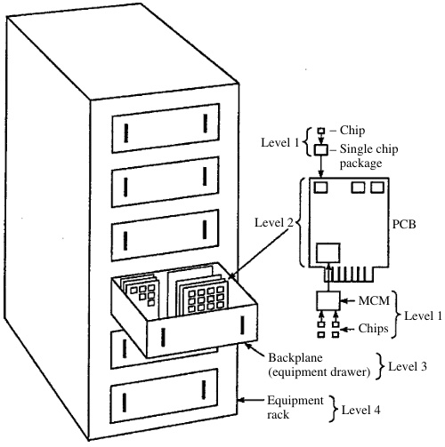
Figure 2.44. Electronic packaging hierarchy.
Overall, electronic systems consist of several levels of packaging, each with distinctive types of interconnection devices. Figure 2.44 depicts this packag ing hierarchy. Level 0 consists of on-chip interconnections. Chip-to-printed cir cuit board or chip-to-module connections constitute level 2, and board-to-board interconnections make up level 3. Levels 4 and 5 consist of connections between subassemblies and between systems (such as computer to printer), respectively.
Die Separation
After functional testing, individual ICs (or dies) must be separated from the substrate. This is the first step in the packaging process. In a common method that has been used for many years, the substrate wafer is mounted on a holder and scribed in both the x and y directions using a diamond scribe. This is done along scribe borders of 75-250 um in width that are formed around the periphery of the dies during fabrication. These borders are aligned with the crystal planes of this substrate if possible. After scribing, the wafer is removed form the holder and placed upside-down on a soft support. A roller is then used to apply pressure, fracturing the wafer along the scribe lines. This must be accomplished with minimal damage to the individual die.
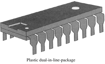
Figure 2.45. Dual-inline package
More modern die separation processes use a diamond saw, rather than a dia mond scribe. In this procedure, the wafer is attached to an adhesive sheet of mylar film. The saw is then used to either scribe the wafer or to cut completely through it. After separation, the dies are removed from the mylar. The separated dice are then ready to be placed into packages.
Package Types
There are a number of approaches to the packaging of single ICs. The dual inline package (DIP) (Figure 2.45), is the package most people envision when they think of integrated circuits. The DIP was developed in the 1960s, quickly became the primary package for ICs, and has long dominated the electronics packaging market. The DIP can be made of plastic or ceramic; the latter is called the CerDIP. The CerDIP consists of a DIP constructed of two pieces of sandwiched ceramic with leads protruding from between the ceramic plates.
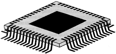
Figure 2.46. Quad flatpack
In the 1970s and 1980s, surface-mount packages were developed in response to a need for higher-density interconnect than the DIP approach could provide. In contrast to DIPs, the leads of a surface-mounted package do not penetrate the printed circuit board (PCB) on which it is mounted. This means that the package can be mounted on both sides of the board, thereby allowing higher density. One example of such a package is the quad flatpack (QFP) (Figure 2.46), which has leads on all four sides to further increase the number of input/output (I/O) connections.
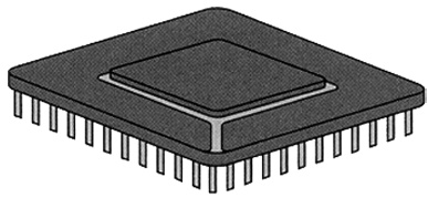
Figure 2.47. Pin-grid array
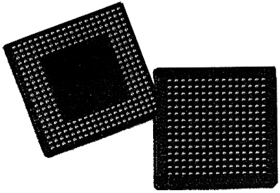
Figure 2.48. Ball-grid array
More recently, the need for rapidly increasing numbers of I/O connections has led to the development of pin-grid array (PGA) and ball-grid array (BGA) packages (Figures 2.47 and 2.48, respectively). PGAs have an I/O density of about 600, and BGAs can have densities greater than 1000, as compared to ˜200 for QFPs. BGAs can be identified by the solder bumps on the bottom of the package. With QFPs, as the spacing between leads becomes tighter, the manufacturing yield decreases rapidly. The BGA allows higher density and takes up less space than the QFP, but its manufacturing process is inherently more expensive.
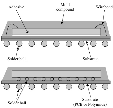
Figure 2.49. Two typical chip-scale packages
The most recent development in packaging is the chip-scale package (CSP), which is shown in Figure 2.49. CSPs, defined as packages no larger than 20% greater than the size of the IC die itself, often take the form of miniaturized ball grid arrays. They are designed to be flipchip-mounted using conventional equipment and solder reflow. CSPs are typically manufactured in a process that creates external power and signal I/O contacts and encapsulates the finished silicon die prior to dicing the wafer. Essentially, CSPs provide an interconnection framework for ICs so that before dicing, each die has all the functions (i.e., external electrical contacts, encapsulation of the finished silicon) of a conventional, fully packaged IC. Two essential features of this approach are that the leads and interposer layer (an added layer on the IC used to provide electrical functionality and mechanical stability) are flexible enough so that the packaged device is compliant with the test fixture for full testing and burning, and the package can accommodate the vertical nonplanarity and thermal expansion and contraction of the underlying printed circuit board during assembly and operation.
Attachment Methods
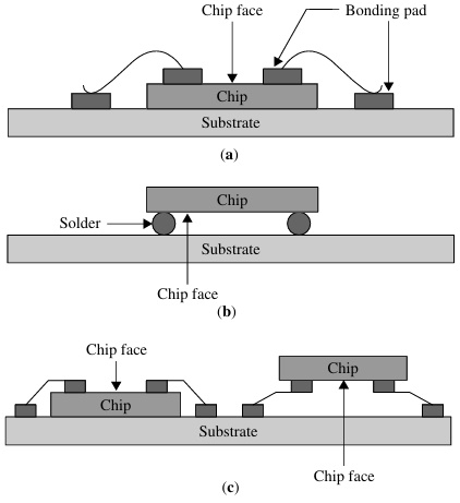
Figure 2.50. (a) Wire; (b) flipchip; (c) tape-automated bonding
An IC must be mounted and bonded to a package, and that package must be attached to a printed circuit board before the IC can be used in an electronic system. Methods of attaching ICs to PCBs are referred to as level 1 packaging. The technique used to bond a bare die to a package has a significant effect on the ultimate electrical, mechanical and thermal properties of electronic system being manufactured. Chip-to-package interconnection is generally accomplished by either wire bonding, tape-automated bonding (TAB), or flipchip bonding (see Figure 2.50).
Wire bonding is the oldest attachment method and is still the dominant tech nique for chips with fewer that 200 I/O connections. Wire bonding requires connecting gold or aluminum wires between chip bonding pads and contact points on the package. ICs are first attached to the substrate using a thermally conduc tive adhesive with their bonding pads facing upward. The Au or Al wires are then attached between the pads and substrate using ultrasonic, thermosonic, or thermocompression bonding. Although automated, this process is still time consuming since each wire must be attached individually.
Tape-automated bonding (TAB) was developed in the early 1970s and is often used to bond packages to PCBs. In TAB, chips are first mounted on a flexi ble polymer tape (usually polyimide) containing repeated copper interconnection patterns. The copper leads are defined by lithography and etching, and the lead pattern can contain hundreds of connections. After the IC pads have been aligned to metal interconnection stripes on the tape, attachment takes place by thermo compression. Gold bumps are formed on either side of the die or tape and are used to bond the die to the leads on the tape.
Flipchip bonding is a direct interconnection approach in which the IC is mounted upside-down onto a module or printed circuit board. Electrical con nections are made via solder bumps (or solderless materials such as epoxies or conductive adhesives) located over the surface of the chip. Since bumps can be located anywhere on the chip, flipchip bonding ensures that the interconnect distance between the chip and package is minimized. The I/O density is limited only by the minimum distance between adjacent bond pads.
This is an excerpt from
Fundamentals of Semiconductor Manufacturing and Process Control by Gary S. May and Costas J. Spanos
A practical guide to semiconductor manufacturing from process control to yield modeling and experimental design. Fundamentals of Semiconductor Manufacturing and Process Control covers all issues involved in manufacturing microelectronic devices and circuits, including fabrication sequences, process control, experimental design, process modeling, yield modeling, and CIM/CAM systems. Readers are introduced to both the theory and practice of all basic manufacturing concepts.
Following an overview of manufacturing and technology, the text explores process monitoring methods, including those that focus on product wafers and those that focus on the equipment used to produce wafers. Next, the text sets forth some fundamentals of statistics and yield modeling, which set the foundation for a detailed discussion of how statistical process control is used to analyze quality and improve yields.
The discussion of statistical experimental design offers readers a powerful approach for systematically varying controllable process conditions and determining their impact on output parameters that measure quality. The authors introduce process modeling concepts, including several advanced process control topics such as run-by-run, supervisory control, and process and equipment diagnosis.
Critical coverage includes the following:
• Combines process control and semiconductor manufacturing
• Unique treatment of system and software technology and management of overall manufacturing systems
• Chapters include case studies, sample problems, and suggested exercises
• Instructor support includes electronic copies of the figures and an instructor's manual
Graduate-level students and industrial practitioners will benefit from the detailed examination of how electronic materials and supplies are converted into finished integrated circuits and electronic products in a high-volume manufacturing environment.
Reader W Boudville says, "For those of you working in a fab, or designing processes to be used in it, May gives a good summary of what is generally known and non-proprietary. He explains the key steps in photolithography, wet and dry etching, the different ways to dope, and deposition processes.
But along with these steps, every fab needs to monitor them for quality control. So we get discussions of how to measure data about a wafer. Like using inteferometry or ellipsometry to measure the thickness of a deposited thin film. Or using a four point probe for capacitance or resistance measurements.
A lot of the text also deals with statistics and how to maximise your device yield. Involves numerous modelling choices and process controls.
Click Here for more information.


