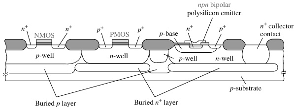
BiCMOS is a technology that combines both CMOS and bipolar device structures in a single IC. The reason to combine these two different technologies is to create an IC chip that has the advantages of both CMOS and bipolar devices. We know that CMOS exhibits advantages in power dissipation, noise margin, and packing density, whereas bipolar technology shows advantages in switching speed, current drive capability, and analog capability. As a result, for a given design rule, BiCMOS can have a higher speed than CMOS, better performance in analog circuits than CMOS, a lower power dissipation than bipolar, and a higher component density than bipolar.

Figure 2.43. BiCMOS device structure
BiCMOS has been widely used in many applications. Early on, it was used in static random access memory (SRAM) circuits. Currently, BiCMOS technology has been successfully developed for transceiver, amplifier, and oscillator applications in wireless communication equipment. Most BiCMOS processes are based on standard CMOS process with some modifications, such as adding masks for bipolar transistor fabrication. The example shown in Figure 2.43 is for a high-performance BiCMOS process based on the twin-well CMOS approach.
The initial material is a p-type silicon substrate. An n+-buried layer is formed to reduce collector resistance. The buried p layer is formed by ion implantation to increase the doping level and prevent punchthrough. A lightly doped n-epi layer is grown on the wafer, and a twin-well process for the CMOS is performed. To achieve high performance for the bipolar transistor, four additional masks are needed: the buried n+ mask, the collector deep n+ mask, the base p mask, and the polyemitter mask. The p+ region for base contact can be formed with the p+ implant in the source-drain implantation of the PMOS, and the n+ emitter can be formed with the source/drain implantation of the NMOS. The additional masks and longer processing time compared with a standard CMOS process are the main drawbacks of BiCMOS.
This is an excerpt from
Fundamentals of Semiconductor Manufacturing and Process Control by Gary S. May and Costas J. Spanos
A practical guide to semiconductor manufacturing from process control to yield modeling and experimental design. Fundamentals of Semiconductor Manufacturing and Process Control covers all issues involved in manufacturing microelectronic devices and circuits, including fabrication sequences, process control, experimental design, process modeling, yield modeling, and CIM/CAM systems. Readers are introduced to both the theory and practice of all basic manufacturing concepts.
Following an overview of manufacturing and technology, the text explores process monitoring methods, including those that focus on product wafers and those that focus on the equipment used to produce wafers. Next, the text sets forth some fundamentals of statistics and yield modeling, which set the foundation for a detailed discussion of how statistical process control is used to analyze quality and improve yields.
The discussion of statistical experimental design offers readers a powerful approach for systematically varying controllable process conditions and determining their impact on output parameters that measure quality. The authors introduce process modeling concepts, including several advanced process control topics such as run-by-run, supervisory control, and process and equipment diagnosis.
Critical coverage includes the following:
• Combines process control and semiconductor manufacturing
• Unique treatment of system and software technology and management of overall manufacturing systems
• Chapters include case studies, sample problems, and suggested exercises
• Instructor support includes electronic copies of the figures and an instructor's manual
Graduate-level students and industrial practitioners will benefit from the detailed examination of how electronic materials and supplies are converted into finished integrated circuits and electronic products in a high-volume manufacturing environment.
Reader W Boudville says, "For those of you working in a fab, or designing processes to be used in it, May gives a good summary of what is generally known and non-proprietary. He explains the key steps in photolithography, wet and dry etching, the different ways to dope, and deposition processes.
But along with these steps, every fab needs to monitor them for quality control. So we get discussions of how to measure data about a wafer. Like using inteferometry or ellipsometry to measure the thickness of a deposited thin film. Or using a four point probe for capacitance or resistance measurements.
A lot of the text also deals with statistics and how to maximise your device yield. Involves numerous modelling choices and process controls.
Click Here for more information.


