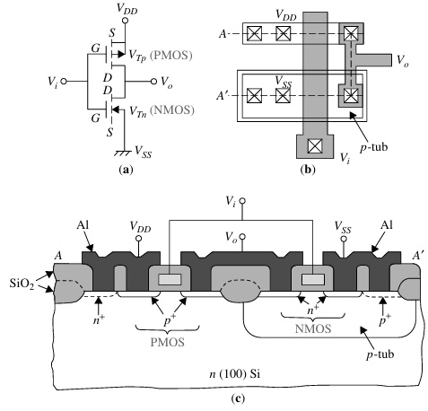
Figure 2.39. CMOS inverter: (a) circuit diagram; (b) layout; and (c) cross section
The MOS process forms the foundation for CMOS technology. Figure 2.39a shows a CMOS inverter. The gate of the upper PMOS device is connected to the gate of the lower NMOS device. For the CMOS inverter, in either logic state, one device in the series path from VDD to ground is nonconductive. The current that flows in either steady state is a small leakage current, and only when both devices are on during switching does a significant current flow through the inverter. Thus, the average power dissipation is on the order of nanowatts. Low power consumption is the most attractive feature of the CMOS circuit.
Figure 2.39b shows a layout of the CMOS inverter, and Figure 2.39c shows the device cross section along the A-A' line. In the processing, a p tub (also called a p well) is first implanted and subsequently driven into the n substrate. The p-type dopant concentration must be high enough to overcompensate the background doping of the n substrate. The subsequent processes for the n-channel MOSFET in the p tub are identical to those described previously. For the p-channel MOSFET, 11B+ or 49(BF2)+ ions are implanted into the n substrate to form the source and drain regions. A channel implant of 75As+ ions may be used to adjust the threshold voltage and a n+ chanstop is formed underneath the field oxide around the p-channel device. Because of the p tub and the additional steps needed to make the p-channel MOSFET, the number of steps to make a CMOS circuit is essentially double that to make an NMOS circuit. Thus, there is a trade-off between the complexity of processing and a reduction in power consumption.

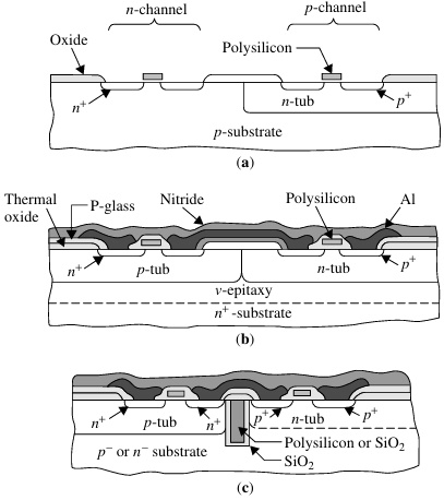
Various CMOS structures: (a) n-tub; (b) twin-tub; (c) refilled trench
Instead of the p tub described above, an alternate approach is to use an n tub formed in p-type substrate, as shown in Figure 2.40a. In this case, the n-type dopant concentration must be high enough to overcompensate for the background doping of the p substrate (i.e., ND > NA). In both the p-tub and the n-tub approaches, the channel mobility will be degraded because mobility is determined by the total dopant concentration (NA + ND). A more recent approach using two separated tubs implanted into a lightly doped substrate is shown in Figure 2.40b. This structure is called a "twin tub." Because no overcompensation is needed in either of the twin tubs, higher channel mobility can be obtained.
All CMOS circuits have the potential for a problem called latchup that is associated with parasitic bipolar transistors. These parasitic devices consist of the npn transistor formed by the NMOS source-drain regions, p tub, and n-type substrate, as well as the pnp transistor formed by the PMOS source-drain regions, n-type substrate, and p tub. Under appropriate conditions, the collector of the pnp device supplies base current to the npn and vice versa in a positive feedback arrangement. This latchup current can have serious negative repercussions in a CMOS circuit.
An effective processing technique to eliminate latchup is to use deep-trench isolation, as shown in Figure 2.40c. In this technique, a trench with a depth deeper than the well is formed in the silicon by anisotropic reactive sputter etching. An oxide layer is thermally grown on the bottom and walls of the trench, which is then refilled by deposited polysilicon or silicon dioxide. This technique can eliminate latchup because the n-channel and p-channel devices are physically isolated by the refilled trench. The detailed steps for trench isolation and some related CMOS processes are now considered.
Well Formation. The well of a CMOS circuit can be a single well, a twin well, or a retrograde well. The twin-well process exhibits some disadvantages. For example, it needs high-temperature processing (above 1050°C) and a long diffusion time (longer than 8 h) to achieve the required well depth of 2-3 um. In this process, the doping concentration is highest at the surface and decreases monotonically with depth. To reduce the process temperature and time, high energy implantation is used (i.e., implanting the ion to the desired depth instead of diffusion from the surface). The profile of the well in this case can have a peak at a certain depth in the silicon substrate. This is called a retrograde well.The advantage of high-energy implantation is that it can form the well under low-temperature and short-time conditions. Hence, it can reduce the lateral diffusion and increase the device density. The retrograde well offers some additional advantages over the conventional well: (1) because of high doping near the bottom, the well resistivity is lower than that of the conventional well, and latchup can be minimized; (2) the chanstop can be formed at the same time as the retro grade well implantation, reducing processing steps and time; and (3) higher well doping in the bottom can reduce the chance of punchthrough from the drain to the source.
Isolation. The conventional MOS isolation process has some disadvantages that make it unsuitable for deep-submicrometer (≤0.25-um) fabrication. The high temperature oxidation of silicon and long oxidation time result in the encroach ment of the chanstop implantation (usually boron for n-MOSFET) to the active region and cause a threshold voltage shift. The area of the active region is reduced because of the lateral oxidation. In addition, the field oxide thickness in submicrometer-isolation spacings is significantly less than the thickness of field oxide grown in wider spacings. Trench isolation technology can avoid these problems.

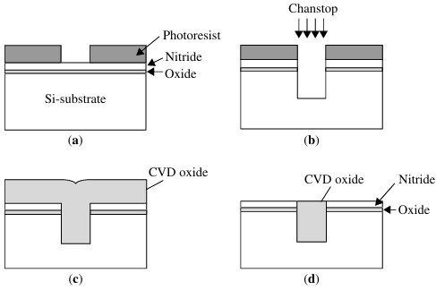
Shallow-trench isolation: (a) patterning on nitride-oxide films; (b) dry etching and
chanstop implantation; (c) CVD oxide to refill; (d) surface after CMP
An example is shallow trench (depth less than 1 um) isolation, shown in Figure 2.41. After patterning (Figure 2.41a), the trench area is etched (Figure 2.41b) and then refilled with oxide (Figure 2.41c). Before refilling, a channel stop implantation can be performed. Since the oxide has overfilled the trench, the oxide on the nitride should be removed. Chemical-mechanical polishing is used to remove the oxide on the nitride and to get a flat surface (Figure 2.41d). Because of its high resistance to polishing, the nitride acts as a stop layer for the CMP process. After the polishing, the nitride layer and the oxide layer can be removed by H3PO4 and HF, respectively. This initial planarization step at the beginning is helpful for the subsequent polysilicon patterning and planarizations of the multilevel interconnection processes.
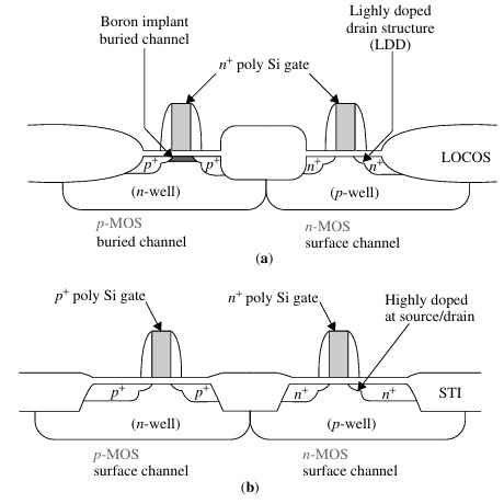
Gate Engineering. If n+-polysilicon is used for both PMOS and NMOS gates, the threshold voltage for PMOS has to be adjusted by boron implantation. This makes the channel of the PMOS a buried type, as shown in Figure 2.42a. The buried-type PMOS suffers serious short-channel effects as the device size shrinks below 0.25 um. The most noticeable phenomena for short-channel effects are threshold voltage rolloff, drain-induced barrier lowering, and the large leakage current at the OFF state. To alleviate these problems, the n+-polysilicon can be changed to p+-polysilicon for the PMOS devices. Due to the workfunction difference (1.0 eV from n+-top+-polysilicon), a surface p-type channel device can be achieved without the boron VT adjustment implantation. Hence, as the technology shrinks to 0.25 um and less, dual-gate structures are required: p+-polysilicon gate for PMOS and n+-polysilicon for NMOS (Figure 2.42b).

Figure 2.42. (a) Conventional CMOS structure with a single polysilicon gate; (b) advanced
CMOSstructure with dual polysilicon gates
To form the p+-polysilicon gate, ion implantation of BF2T shift. This penetration is enhanced in the presence of a F atom. There are methods to reduce this effect: use of rapid thermal annealing to reduce the time at high temperatures and, consequently, the diffusion of boron; use of nitrided oxide to suppress the boron penetration, since boron can easily combine with nitrogen and becomes less mobile; and the creation of a multilayer of polysilicon to trap the boron atoms at the interface of the two layers.
This is an excerpt from
Fundamentals of Semiconductor Manufacturing and Process Control by Gary S. May and Costas J. Spanos
A practical guide to semiconductor manufacturing from process control to yield modeling and experimental design. Fundamentals of Semiconductor Manufacturing and Process Control covers all issues involved in manufacturing microelectronic devices and circuits, including fabrication sequences, process control, experimental design, process modeling, yield modeling, and CIM/CAM systems. Readers are introduced to both the theory and practice of all basic manufacturing concepts.
Following an overview of manufacturing and technology, the text explores process monitoring methods, including those that focus on product wafers and those that focus on the equipment used to produce wafers. Next, the text sets forth some fundamentals of statistics and yield modeling, which set the foundation for a detailed discussion of how statistical process control is used to analyze quality and improve yields.
The discussion of statistical experimental design offers readers a powerful approach for systematically varying controllable process conditions and determining their impact on output parameters that measure quality. The authors introduce process modeling concepts, including several advanced process control topics such as run-by-run, supervisory control, and process and equipment diagnosis.
Critical coverage includes the following:
• Combines process control and semiconductor manufacturing
• Unique treatment of system and software technology and management of overall manufacturing systems
• Chapters include case studies, sample problems, and suggested exercises
• Instructor support includes electronic copies of the figures and an instructor's manual
Graduate-level students and industrial practitioners will benefit from the detailed examination of how electronic materials and supplies are converted into finished integrated circuits and electronic products in a high-volume manufacturing environment.
Reader W Boudville says, "For those of you working in a fab, or designing processes to be used in it, May gives a good summary of what is generally known and non-proprietary. He explains the key steps in photolithography, wet and dry etching, the different ways to dope, and deposition processes.
But along with these steps, every fab needs to monitor them for quality control. So we get discussions of how to measure data about a wafer. Like using inteferometry or ellipsometry to measure the thickness of a deposited thin film. Or using a four point probe for capacitance or resistance measurements.
A lot of the text also deals with statistics and how to maximise your device yield. Involves numerous modelling choices and process controls.
Click Here for more information.


