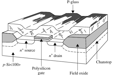
Figure 2.36. n-channel MOSFET
The MOSFET is the dominant device used in modern integrated circuits because it can be scaled to smaller dimensions than other types of devices. The dominant technology for MOSFET is complementary MOSFET (CMOS) technology, in which both n-channel and p-channel devices (NMOS and PMOS, respectively) are provided on the same chip. CMOS technology is particular attractive because it has the lowest power consumption of all IC technology. Figure 2.36 shows a perspective view of an n-channel MOSFET prior to final metallization. The top layer is a phosphorus-doped silicon dioxide (P-glass) that is used as an insulator between the polysilicon gate and the gate metallization and also as a gettering layer for mobile ions.
Basic NMOS Fabrication Sequence

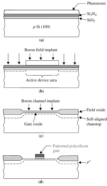
Figure 2.37. NNMOS fabrication sequence: (a) formation of SiO2, Si3N4, and photoresist layers;
(b) boron implant; (c) field oxide; (d) gate
In an NMOS process, the starting material is a p-type, lightly doped (≈1015 cm-3), {100}-oriented, polished silicon wafer. The first step is to form the oxide isolation region using LOCOS technology. The process sequence for this step is similar to that for the bipolar transistor. A thin-pad oxide (≈35 nm) is thermally grown, followed by a silicon nitride (≈150 nm) deposition (Figure 2.37a). The active-device area is defined by a photoresist mask and a boron chanstop layer and is then implanted through the composite nitride-oxide layer (Figure 2.37b). The nitride layer not covered by the photoresist mask is subsequently removed by etching. After stripping the photoresist, the wafer is placed in an oxidation furnace to grow an oxide (called the field oxide), where the nitride layer is removed, and to drive in the boron implant. The thickness of the field oxide is typically 0.5-1 um.
The second step is to grow the gate oxide and to adjust the threshold voltage. The composite nitride-oxide layer over the active-device area is removed, and a thin-gate oxide layer (less than 10 nm) is grown. For an enhancement-mode n-channel device, boron ions are implanted in the channel region, as shown in Figure 2.37c, to increase the threshold voltage to a predetermined value (e.g., +0.5 V). For a depletion-mode n-channel device, arsenic ions are implanted in the channel region to decrease the threshold voltage (e.g., -0.5 V).
The third step is to form the gate. A polysilicon is deposited and is heavily doped by diffusion or implantation of phosphorus to a typical sheet resistance of 20-30 Ω/[]. This resistance is adequate for MOSFETs with gate lengths larger than 3 um. For smaller devices, polycide, a composite layer of metal silicide and polysilicon such as W-polycide, can be used as the gate materials to reduce the sheet resistance to about 1 Ω/[].

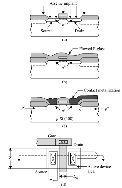
Figure 2.38. NMOS fabrication sequence: (a) source and drain; (b) P-glass deposition;
(c) MOSFET cross section; (d) MOSFET top view
The fourth step is to form the source and drain. After the gate is patterned (Figure 2.37d), it serves as a mask for the arsenic implantation (≈30 keV, ≈5 x 1015 cm−2) to form the source and drain (Figure 2.38a), which are self-aligned with respect to the gate. At this stage, the only overlapping of the gate is due to lateral straggling of the implanted ions (for 30 keV As, ω U+253x is only 5 nm). If low-temperature processes are used for subsequent steps to minimize lateral diffusion, the parasitic gate-drain and gate-source coupling capacitances can be much smaller than the gate-channel capacitance.
The last step is metallization. P-glass is deposited over the entire wafer and is flowed by heating the wafer to give a smooth surface topography (Figure 2.38b). Contact windows are defined and etched in the P-glass. A metal layer, such as aluminum, is then deposited and patterned. A cross-sectional view of the completed MOSFET is shown in Figure 2.38c, and the corresponding top view is shown in Figure 2.38d. The gate contact is usually made outside the active-device area to avoid possible damage to the thin-gate oxide.
This is an excerpt from
Fundamentals of Semiconductor Manufacturing and Process Control by Gary S. May and Costas J. Spanos
A practical guide to semiconductor manufacturing from process control to yield modeling and experimental design. Fundamentals of Semiconductor Manufacturing and Process Control covers all issues involved in manufacturing microelectronic devices and circuits, including fabrication sequences, process control, experimental design, process modeling, yield modeling, and CIM/CAM systems. Readers are introduced to both the theory and practice of all basic manufacturing concepts.
Following an overview of manufacturing and technology, the text explores process monitoring methods, including those that focus on product wafers and those that focus on the equipment used to produce wafers. Next, the text sets forth some fundamentals of statistics and yield modeling, which set the foundation for a detailed discussion of how statistical process control is used to analyze quality and improve yields.
The discussion of statistical experimental design offers readers a powerful approach for systematically varying controllable process conditions and determining their impact on output parameters that measure quality. The authors introduce process modeling concepts, including several advanced process control topics such as run-by-run, supervisory control, and process and equipment diagnosis.
Critical coverage includes the following:
• Combines process control and semiconductor manufacturing
• Unique treatment of system and software technology and management of overall manufacturing systems
• Chapters include case studies, sample problems, and suggested exercises
• Instructor support includes electronic copies of the figures and an instructor's manual
Graduate-level students and industrial practitioners will benefit from the detailed examination of how electronic materials and supplies are converted into finished integrated circuits and electronic products in a high-volume manufacturing environment.
Reader W Boudville says, "For those of you working in a fab, or designing processes to be used in it, May gives a good summary of what is generally known and non-proprietary. He explains the key steps in photolithography, wet and dry etching, the different ways to dope, and deposition processes.
But along with these steps, every fab needs to monitor them for quality control. So we get discussions of how to measure data about a wafer. Like using inteferometry or ellipsometry to measure the thickness of a deposited thin film. Or using a four point probe for capacitance or resistance measurements.
A lot of the text also deals with statistics and how to maximise your device yield. Involves numerous modelling choices and process controls.
Click Here for more information.


