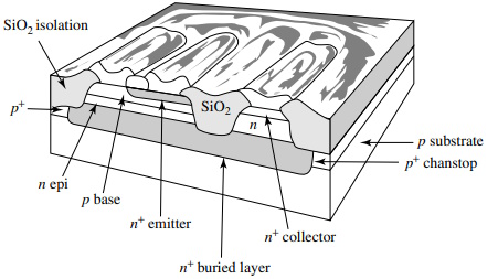
Figure 2.32. Oxide-isolated bipolar transistor.
The majority of bipolar transistors used in ICs are of the n-p-n type because the higher mobility of minority carriers (electrons) in the base region results in higher speed performance than can be obtained with p-n-p types. Figure 2.32 shows a perspective view of an n-p-n bipolar transistor in which lateral isolation is provided by oxide walls and vertical isolation is provided by the n+ -p junction. The lateral oxide isolation approach reduces not only the device size but also the parasitic capacitance because of the smaller dielectric constant of silicon dioxide (3.9, compared with 11.9 for silicon).
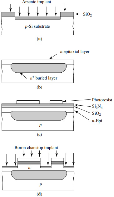
For an n-p-n bipolar transistor, the starting material is a p-type, lightly doped (˜1015 cm-3), (111) - or (100)-oriented, polished silicon wafer. Because the junctions are formed inside the semiconductor, the choice of crystal orientation is not as critical as for MOS devices. The first step is to form a buried layer. The main purpose of this layer is to minimize the series resistance of the collector. A thick oxide (0.5-1 um) is thermally grown on the wafer, and a window is then opened in the oxide. A precisely controlled amount of low-energy arsenic ions (˜30 keV, ˜1015 cm-2) is implanted into the window region to serve as a predeposit (Figure 2.33a). Next, a high-temperature (˜1100°C) drive-in step forms the n+-buried layer, which has a typical sheet resistance of 20 Ω/[].

Figure 2.33. Cross-sectional views of bipolar transistor fabrication: (a) buried-layer
implantation; (b) epitaxial layer; (c) photoresist mask; (d) channel-stop layer.
The second step is to deposit an n-type epitaxial layer. The oxide is removed and the wafer is placed in an epitaxial reactor for epitaxial growth. The thickness and the doping concentration of the epitaxial layer are determined by the ultimate use of the device. Analog circuits (with their higher voltages for amplification) require thicker layers (˜10 um) and lower dopings (˜5 × 1015 cm-3), whereas digital circuits (with their lower voltages for switching) require thinner layers (˜3 um) and higher dopings (˜2 × 1016 cm-3). Figure 2.33b shows a crosssectional view of the device after the epitaxial process.
The third step is to form the lateral oxide isolation region. A thin oxide pad (˜50 nm) is thermally grown on the epitaxial layer, followed by a silicon nitride deposition (˜100 nm). If nitride is deposited directly onto the silicon without the thin oxide pad, the nitride may cause damage to the silicon surface during subsequent high-temperature steps. Next, the nitride-oxide layers and about half of the epitaxial layer are etched using a photoresist as mask (Figures 2.33c and 2.33d). Boron ions are then implanted into the exposed silicon areas (Figure 2.33d).

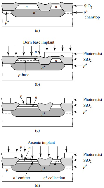
Figure 2.34. Cross-sectional views of bipolar transistor fabrication: (a) oxide isolation; (b) base
implantation; (c) removal of thin oxide; (d) emitter-collector implant.
The photoresist is removed, and the wafer is placed in an oxidation furnace. Since the nitride layer has a very low oxidation rate, thick oxides will be grown only in the areas not protected by the nitride layer. The isolation oxide is usually grown to a thickness such that the top of the oxide becomes coplanar with the original silicon surface to minimize the surface topography. This oxide isolation process is called local oxidation of silicon (LOCOS). Figure 2.34a shows the cross section of the isolation oxide after removal of the nitride layer. Because of segregation effects, most of the implanted boron ions are pushed underneath the isolation oxide to form a p+ layer. This is called the p+-channel stop (or chanstop), because the high concentration of p-type semiconductor will prevent surface inversion and eliminate possible high-conductivity paths (or channels) among neighboring buried layers.
The fourth step is to form the base region. A photoresist is used as a mask to protect the right half of the device. Then, boron ions (˜1012 cm-2) are implanted to form the base regions, as shown in Figure 2.34b. Another lithographic process removes all the thin pad oxide except for a small area near the center of the base region (Figure 2.34c). The fifth step is to form the emitter region. As shown in Figure 2.34d, the base contact area is protected by a photoresist mask. Then, a low-energy, high-arsenic-dose (˜1016 cm-2) implantation forms the n+-emitter and n+-collector contact regions. The photoresist is removed, and a final metallization step forms the contacts to the base, emitter, and collector, as shown in Figure 2.32.
In this basic bipolar process, there are six film formation operations, six lithographic operations, four ion implantations, and four etching operations. Each operation must be precisely controlled and monitored. Failure of any one of the operations generally will render the wafer useless. The doping profiles of the completed transistor along a coordinate perpendicular to the surface and passing through the emitter, base, and collector are shown in Figure 2.35. The emitter profile is abrupt because of the concentration-dependent diffusivity of arsenic. The base doping profile beneath the emitter can be approximated by a Gaussian distribution for limited-source diffusion. The collector doping is given by the epitaxial doping level (˜2 x 1016 cm-3) for a representative switching transistor.
This is an excerpt from
Fundamentals of Semiconductor Manufacturing and Process Control by Gary S. May and Costas J. Spanos
A practical guide to semiconductor manufacturing from process control to yield modeling and experimental design. Fundamentals of Semiconductor Manufacturing and Process Control covers all issues involved in manufacturing microelectronic devices and circuits, including fabrication sequences, process control, experimental design, process modeling, yield modeling, and CIM/CAM systems. Readers are introduced to both the theory and practice of all basic manufacturing concepts.
Following an overview of manufacturing and technology, the text explores process monitoring methods, including those that focus on product wafers and those that focus on the equipment used to produce wafers. Next, the text sets forth some fundamentals of statistics and yield modeling, which set the foundation for a detailed discussion of how statistical process control is used to analyze quality and improve yields.
The discussion of statistical experimental design offers readers a powerful approach for systematically varying controllable process conditions and determining their impact on output parameters that measure quality. The authors introduce process modeling concepts, including several advanced process control topics such as run-by-run, supervisory control, and process and equipment diagnosis.
Critical coverage includes the following:
• Combines process control and semiconductor manufacturing
• Unique treatment of system and software technology and management of overall manufacturing systems
• Chapters include case studies, sample problems, and suggested exercises
• Instructor support includes electronic copies of the figures and an instructor's manual
Graduate-level students and industrial practitioners will benefit from the detailed examination of how electronic materials and supplies are converted into finished integrated circuits and electronic products in a high-volume manufacturing environment.
Reader W Boudville says, "For those of you working in a fab, or designing processes to be used in it, May gives a good summary of what is generally known and non-proprietary. He explains the key steps in photolithography, wet and dry etching, the different ways to dope, and deposition processes.
But along with these steps, every fab needs to monitor them for quality control. So we get discussions of how to measure data about a wafer. Like using inteferometry or ellipsometry to measure the thickness of a deposited thin film. Or using a four point probe for capacitance or resistance measurements.
A lot of the text also deals with statistics and how to maximise your device yield. Involves numerous modelling choices and process controls.
Click Here for more information.


