An integrated circuit is an ensemble of active (e.g., transistors) and passive devices (e.g., resistors, capacitors, and inductors) formed on and within a single-crystal semiconductor substrate and interconnected by a metallization pattern.
ICs have enormous advantages over discrete devices, including (1) reduction of the interconnection parasitics, (2) full utilization of a semiconductor wafer's area, and (3) drastic reduction in processing cost. In this article, we discuss the manner in which the basic processes are combined to fabricate ICs.
We consider three major IC technologies associated with two transistor families (viz., bipolar junction transistors and metal-oxide-semiconductor field-effect transistors, or MOSFETs): bipolar, CMOS, and BiCMOS. BiCMOS (Bipolar CMOS) is a technology that integrates two semiconductor technologies, those of the bipolar junction transistor and the CMOS logic gate, into a single integrated circuit.
The majority of bipolar transistors used in ICs are of the n-p-n type because the higher mobility of minority carriers (electrons) in the base region results in higherspeed performance than can be obtained with p-n-p types.
The MOSFET is the dominant device used in modern integrated circuits because it can be scaled to smaller dimensions than other types of devices. The dominant technology for MOSFET is complementary MOSFET (CMOS) technology, in which both n-channel and p-channel devices (NMOS and PMOS, respectively) are provided on the same chip.

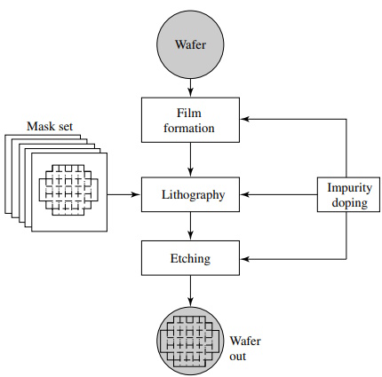
Figure 2.30. Schematic diagram of IC fabrication
Figure 2.30 illustrates the interrelationship between the major process steps used for IC fabrication. Polished wafers with a specific resistivity and orientation are used as the starting material. The film formation steps include thermally grown. oxide films, deposited polysilicon, dielectric, and metal films. Film formation is often followed by lithography or impurity doping. Lithography is generally followed by etching, which in turn is often followed by another impurity doping or film formation. The final IC is made by sequentially transferring the patterns from each mask, level by level, onto the surface of the semiconductor wafer.

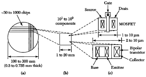
Figure 2.31. (a) Semiconductor wafer; (b) IC chip; (c) MOSFET and bipolar transistor
After processing, each wafer contains hundreds of identical rectangular chips (or dies), typically between 1 and 20 mm on each side, as shown in Figure 2.31a. The chips are separated by sawing or laser cutting. Figure 2.31b shows a separated chip. Schematic top views of a single MOSFET and a single bipolar transistor are shown in Figure 2.31c to give some perspective of the relative size of a component in an IC chip. Prior to chip separation, each chip is electrically tested. Good chips are selected and packaged to provide an appropriate thermal, electrical, and interconnection environment for electronic applications.
This is an excerpt from
Fundamentals of Semiconductor Manufacturing and Process Control by Gary S. May and Costas J. Spanos
A practical guide to semiconductor manufacturing from process control to yield modeling and experimental design. Fundamentals of Semiconductor Manufacturing and Process Control covers all issues involved in manufacturing microelectronic devices and circuits, including fabrication sequences, process control, experimental design, process modeling, yield modeling, and CIM/CAM systems. Readers are introduced to both the theory and practice of all basic manufacturing concepts.
Following an overview of manufacturing and technology, the text explores process monitoring methods, including those that focus on product wafers and those that focus on the equipment used to produce wafers. Next, the text sets forth some fundamentals of statistics and yield modeling, which set the foundation for a detailed discussion of how statistical process control is used to analyze quality and improve yields.
The discussion of statistical experimental design offers readers a powerful approach for systematically varying controllable process conditions and determining their impact on output parameters that measure quality. The authors introduce process modeling concepts, including several advanced process control topics such as run-by-run, supervisory control, and process and equipment diagnosis.
Critical coverage includes the following:
• Combines process control and semiconductor manufacturing
• Unique treatment of system and software technology and management of overall manufacturing systems
• Chapters include case studies, sample problems, and suggested exercises
• Instructor support includes electronic copies of the figures and an instructor's manual
Graduate-level students and industrial practitioners will benefit from the detailed examination of how electronic materials and supplies are converted into finished integrated circuits and electronic products in a high-volume manufacturing environment.
Reader W Boudville says, "For those of you working in a fab, or designing processes to be used in it, May gives a good summary of what is generally known and non-proprietary. He explains the key steps in photolithography, wet and dry etching, the different ways to dope, and deposition processes.
But along with these steps, every fab needs to monitor them for quality control. So we get discussions of how to measure data about a wafer. Like using inteferometry or ellipsometry to measure the thickness of a deposited thin film. Or using a four point probe for capacitance or resistance measurements.
A lot of the text also deals with statistics and how to maximise your device yield. Involves numerous modelling choices and process controls.
Click Here for more information.


