Many different types of thin films are used to manufacture integrated circuits, including thermal oxides, dielectric layers, epitaxial layers, polycrystalline silicon, and metal films. This article addresses two of the various techniques for depositing such films: physical vapor deposition and chemical vapor deposition.
Physical Vapor Deposition
The most common methods of physical vapor deposition (PVD) of metals are evaporation, electron-beam evaporation, plasma spray deposition, and sputtering. Metals and metal compounds can be deposited by PVD. Evaporation occurs when a source material is heated above its melting point in an evacuated chamber. The evaporated atoms then travel at high velocity in straight-line trajectories. The source can be melted by resistance heating, by radio frequency (RF) heating, or with a focused electron beam (or e-beam). Evaporation and e-beam evaporation were used extensively in earlier generations of integrated circuits, but they have been replaced by sputtering for modern ICs.

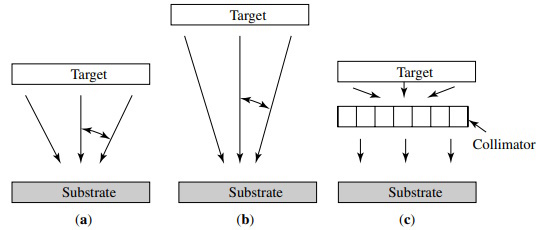
Figure 2.27. (a) Standard sputtering; (b) long-throw sputtering; (c) sputtering
through a collimator
In ion-beam sputtering, a source of ions is accelerated toward the target and impinges on its surface. Figure 2.27a shows a standard sputtering system. The sputtered material deposits on a wafer that is placed facing the target. The ion current and energy can be independently adjusted. Since the target and wafer are placed in a chamber that has lower pressure, more target material and less contamination are transferred to the wafer.
One method to increase the deposition rate in sputtering is to use a third electrode that provides more electrons for ionization. Another method is to use a magnetic field, such as in electron cyclotron resonance (ECR) systems, to capture and spiral electrons, increasing their ionizing efficiency in the vicinity of the sputtering target. This technique, referred to as magnetron sputtering, has found widespread applications for the deposition of aluminum and its alloys at a rate that can approach 1 um/min.
Long-throw sputtering is another technique used to control the angular distribution. Figure 2.27b shows a long-throw sputtering system. In standard sputtering configurations, there are two primary reasons for a wide angular distribution of incident flux at the surface: (1) the use of a small target to substrate separation dts and (2) scattering of the flux by the working gas as the flux travels from the target to the substrate. These two factors are linked because a small dts is needed to achieve good throughput, uniformity, and film properties when there is substantial gas scattering.
A solution to this problem is to sputter at very low pressures, a capability that has been developed using a variety of systems, which can sustain the magnetron plasma under more rarefied conditions. These systems allow for sputtering at working pressures of less than 0.1 Pa. At these pressures, gas scattering is less important, and the target-substrate distance can be greatly increased. From a simple geometric argument, this allows the angular distribution to be greatly narrowed, which permits more deposition at the bottom of high-aspect features such as contact holes.
Contact holes with large aspect ratio are difficult to fill with material, mainly because scattering events cause the top opening of the hole to seal before appreciable material has deposited on its floor. This problem can be overcome by collimating the sputtered atoms by placing an array of collimating tubes just above the wafer to restrict the depositing flux to normal ±5°. Sputtering with a collimator is shown in Figure 2.27c. Atoms whose trajectory is more than 5° from normal are deposited on the inner surface of the collimators.
Chemical Vapor Deposition

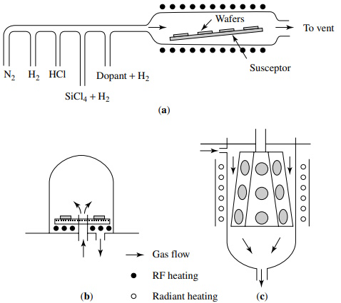
Figure 2.28. Common susceptors for CVD: (a) horizontal; (b) pancake; (c) barrel
Chemical vapor deposition (CVD), also known as vapor-phase epitaxy (VPE), is a process whereby an epitaxial layer is formed by a chemical reaction between gaseous compounds. CVD can be performed at atmospheric pressure (APCVD) or at low pressure (LPCVD). Figure 2.28 shows three common susceptors for epitaxial growth. Note that the geometric shape of the susceptor provides the name for the reactor: horizontal, pancake, and barrel susceptors-all made from graphite blocks. Susceptors in epitaxial reactors are analogous to crucibles in the crystal growing furnaces. Not only do they mechanically support the wafer, but in induction-heated reactors, they also serve as the source of thermal energy for the reaction. The mechanism of CVD involves a number of steps: (1) the reactants (gases and dopants) are transported to the substrate region; (2) they are transferred to the substrate surface, where they are adsorbed; (3) a chemical reaction occurs, catalyzed at the surface, followed by growth of the epitaxial layer; (4) the gaseous products are desorbed into the main gas stream; and (5) the reaction products are transported out of the reaction chamber.

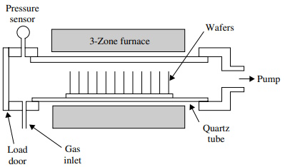
Figure 1.14. Example of a batch process: a CVD reactor
CVD is attractive for metallization because it offers coatings that are conformal, has good step coverage, and can coat a large number of wafers at a time. The basic CVD setup is the same as that used for deposition of dielectrics and polysilicon (see Figure 1.14). Low-pressure CVD (LPCVD) is capable of producing conformal step coverage over a wide range of topographical profiles, often with lower electrical resistivity than that from PVD. One of the major new applications of CVD metal deposition for integrated circuit production is in the area of refractory metal deposition. For example, tungsten’s low electrical resistivity (5.3 u Ω x cm) and refractory nature make it a desirable metal for use in IC fabrication.
Planarization
The development of chemical–mechanical polishing (CMP) has become important for multilevel interconnection technology because it is the only method that allows global planarization (i.e., a flat surface across the whole wafer). It also offers other advantages, including reduced defect density and the avoidance of plasma damage (which would occur in an RIE-based planarization system).

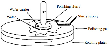
Figure 2.29. CMP schematic
The CMP process consists of moving the sample surface against a pad that carries slurry between the sample surface and the pad. Abrasive particles in the slurry cause mechanical damage on the sample surface, loosening the material for enhanced chemical attack or fracturing off the pieces of surface into a slurry where they dissolve or are swept away. The process is tailored to provide an enhanced material removal rate from high points on surfaces. Mechanical grinding alone may theoretically achieve the desired planarization, but is undesirable because of extensive associated damage to the material surface. There are three main parts of the process: (1) the surface to be polished; (2) the pad, which is the key medium enabling the transfer of mechanical action to the surface being polished; and (3) the slurry, which provides both chemical and mechanical effects. Figure 2.29 shows a typical CMP setup.
This is an excerpt from
Fundamentals of Semiconductor Manufacturing and Process Control by Gary S. May and Costas J. Spanos
A practical guide to semiconductor manufacturing from process control to yield modeling and experimental design. Fundamentals of Semiconductor Manufacturing and Process Control covers all issues involved in manufacturing microelectronic devices and circuits, including fabrication sequences, process control, experimental design, process modeling, yield modeling, and CIM/CAM systems. Readers are introduced to both the theory and practice of all basic manufacturing concepts.
Following an overview of manufacturing and technology, the text explores process monitoring methods, including those that focus on product wafers and those that focus on the equipment used to produce wafers. Next, the text sets forth some fundamentals of statistics and yield modeling, which set the foundation for a detailed discussion of how statistical process control is used to analyze quality and improve yields.
The discussion of statistical experimental design offers readers a powerful approach for systematically varying controllable process conditions and determining their impact on output parameters that measure quality. The authors introduce process modeling concepts, including several advanced process control topics such as run-by-run, supervisory control, and process and equipment diagnosis.
Critical coverage includes the following:
• Combines process control and semiconductor manufacturing
• Unique treatment of system and software technology and management of overall manufacturing systems
• Chapters include case studies, sample problems, and suggested exercises
• Instructor support includes electronic copies of the figures and an instructor's manual
Graduate-level students and industrial practitioners will benefit from the detailed examination of how electronic materials and supplies are converted into finished integrated circuits and electronic products in a high-volume manufacturing environment.
Reader W Boudville says, "For those of you working in a fab, or designing processes to be used in it, May gives a good summary of what is generally known and non-proprietary. He explains the key steps in photolithography, wet and dry etching, the different ways to dope, and deposition processes.
But along with these steps, every fab needs to monitor them for quality control. So we get discussions of how to measure data about a wafer. Like using inteferometry or ellipsometry to measure the thickness of a deposited thin film. Or using a four point probe for capacitance or resistance measurements.
A lot of the text also deals with statistics and how to maximise your device yield. Involves numerous modelling choices and process controls.
Click Here for more information.


