Impurity doping is the introduction of controlled amounts of impurities into semiconductors to change their electrical properties. Diffusion and ion implantation are the two key methods of impurity doping. Both diffusion and ion implantation are used for fabricating discrete devices and integrated circuits because these processes generally complement each other. For example, diffusion is used to form a deep junction (e.g., a twin well in CMOS), whereas ion implantation is used to form a shallow junction (e.g., a source–drain junction of a MOSFET).

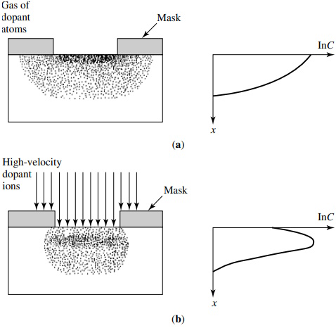
Until the early 1970s, impurity doping was performed by diffusion at elevated temperatures, as shown in Figure 2.22a. In this method the dopant atoms are placed on or near the surface of the wafer by deposition from the gas phase of the dopant or by using doped-oxide sources. The doping concentration decreases monotonically from the surface, and the profile of the dopant distribution is determined mainly by the temperature and the diffusion time. Since the 1970s, doping operations have been performed chiefly by ion implantation, as shown in Figure 2.22b. In this process the dopant ions are implanted into the semiconductor by means of an ion beam. The doping concentration has a peak distribution inside the semiconductor, and the profile of the dopant distribution is determined mainly by the ion mass and the implanted ion energy.
Diffusion of Impurities
Diffusion of impurities is accomplished by placing semiconductor wafers in a carefully controlled, high-temperature quartz-tube furnace and passing a gas mixture that contains the desired dopant through it. The number of dopant atoms that diffuse into the semiconductor is related to the partial pressure of the dopant impurity in the gas mixture. For diffusion in silicon, boron is the most popular dopant for introducing a p-type impurity, whereas arsenic and phosphorus are used extensively as n-type dopants. These dopants can be introduced in several ways, including solid sources (e.g., BN for boron, As2O3 for arsenic, and P2O5 for phosphorus), liquid sources (BBr3, AsCl3, and POCl3), and gaseous sources (B2H6, AsH3, and PH3). However, liquid sources are most commonly used.
Ion Implantation
Since the early 1970s, many doping operations have been performed by ion implantation, which is shown in Figure 2.22b. In this process the energetic dopant ions are implanted into the semiconductor by means of an ion beam. The doping concentration has a peak distribution inside the semiconductor and the profile of the dopant distribution is determined mainly by the ion mass and energy.
Implantation energies are typically between 1 keV and 1 MeV, resulting in ion distributions with average depths ranging from 10 nm to 10 um. Ion doses vary from 1012 ions/cm2 for threshold voltage adjustment in MOSFETs to 1018 ions/cm2 for the formation of buried insulating layer. Note that the dose is expressed as the number of ions implanted into 1 cm2 of the semiconductor surface area. The main advantages of ion implantation are its more precise control and reproducibility of impurity dopings and its lower processing temperature compared with those of the diffusion process.
This is an excerpt from
Fundamentals of Semiconductor Manufacturing and Process Control by Gary S. May and Costas J. Spanos
A practical guide to semiconductor manufacturing from process control to yield modeling and experimental design. Fundamentals of Semiconductor Manufacturing and Process Control covers all issues involved in manufacturing microelectronic devices and circuits, including fabrication sequences, process control, experimental design, process modeling, yield modeling, and CIM/CAM systems. Readers are introduced to both the theory and practice of all basic manufacturing concepts.
Following an overview of manufacturing and technology, the text explores process monitoring methods, including those that focus on product wafers and those that focus on the equipment used to produce wafers. Next, the text sets forth some fundamentals of statistics and yield modeling, which set the foundation for a detailed discussion of how statistical process control is used to analyze quality and improve yields.
The discussion of statistical experimental design offers readers a powerful approach for systematically varying controllable process conditions and determining their impact on output parameters that measure quality. The authors introduce process modeling concepts, including several advanced process control topics such as run-by-run, supervisory control, and process and equipment diagnosis.
Critical coverage includes the following:
• Combines process control and semiconductor manufacturing
• Unique treatment of system and software technology and management of overall manufacturing systems
• Chapters include case studies, sample problems, and suggested exercises
• Instructor support includes electronic copies of the figures and an instructor's manual
Graduate-level students and industrial practitioners will benefit from the detailed examination of how electronic materials and supplies are converted into finished integrated circuits and electronic products in a high-volume manufacturing environment.
Reader W Boudville says, "For those of you working in a fab, or designing processes to be used in it, May gives a good summary of what is generally known and non-proprietary. He explains the key steps in photolithography, wet and dry etching, the different ways to dope, and deposition processes.
But along with these steps, every fab needs to monitor them for quality control. So we get discussions of how to measure data about a wafer. Like using inteferometry or ellipsometry to measure the thickness of a deposited thin film. Or using a four point probe for capacitance or resistance measurements.
A lot of the text also deals with statistics and how to maximise your device yield. Involves numerous modelling choices and process controls.
Click Here for more information.


