photolithography is the process of transferring patterns to photoresist covering the surface of a semiconductor wafer. To produce circuit features, these resist patterns must be transferred into the underlying layers of the device. Pattern transfer is accomplished by an etching process that selectively removes unmasked portions of a layer.
Wet Chemical Etching
Wet chemical etching is used extensively in semiconductor processing. Prior to thermal oxidation or epitaxial growth, semiconductor wafers are chemically cleaned to remove contamination that results from handling and storing. Wet chemical etching is especially suitable for blanket etches (i.e., over the whole wafer surface) of polysilicon, oxide, nitride, metals, and III–V compounds.

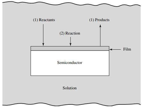
Figure 2.18. Basic mechanisms in wet chemical etching
The mechanisms for wet chemical etching involve three essential steps, as illustrated in Figure 2.18; the reactants are transported by diffusion (the movement of molecules from an area of higher concentration to an area of lower concentration) to the reacting surface, chemical reactions occur at the surface, and the products from the surface are removed by diffusion. Both agitation and the temperature of the etchant solution will influence the etch rate, which is the amount of film removed by etching per unit time. In IC processing, most wet chemical etches proceed by immersing the wafers in a chemical solution or by spraying the wafers with the etchant solution. For immersion etching, the wafer is immersed in the etch solution, and mechanical agitation is usually required to ensure etch uniformity and a consistent etch rate. Spray etching has gradually replaced immersion etching because it greatly increases the etch rate and uniformity by constantly supplying fresh etchant to the wafer surface.
In semiconductor production lines, highly uniform etch rates are important. Etch rates must be uniform across a wafer, from wafer to wafer, from run to run, and for any variations in feature sizes and pattern densities. Etch rate uniformity is given by
(formula 2.20)Dry Etching

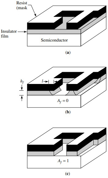
Figure 2.19. Comparison between wet and dry etching: (a) resist pattern; (b) isotropic etching;
(c) anisotropic etching
In pattern transfer operations, a resist pattern is defined by a photolithographic process to serve as a mask for etching of its underlying layer (Figure 2.19a). Most of the layer materials (e.g., SiO2, Si3N4, and deposited metals) are amorphous or polycrystalline thin films. If they are etched in a wet etchant, the etch rate is generally isotropic (i.e., the lateral and vertical etch rates are the same), as illustrated in Figure 2.19b. If hf is the thickness of the layer material and l the lateral distance etched underneath the resist mask, we can define the degree of anisotropy (Af) by
(formula 2.21)where t is time and Rl and Rv are the lateral and vertical etch rates, respectively. For isotropic etching, Rl = Rv and Af = 0.
The major disadvantage of wet etching in pattern transfer is the undercutting of the layer underneath the mask, resulting in a loss of resolution in the etched pattern. In practice, for isotropic etching, the film thickness should be about one third or less of the resolution required. If patterns are required with resolutions much smaller than the film thickness, anisotropic etching (i.e., 1 ≥ Af > 0) must be used. In practice, the value of Af is chosen to be close to unity. Figure 2.19c shows the limiting case where Af = 1, corresponding to l = 0 (or R1 = 0).
To achieve a high-fidelity transfer of the resist patterns required for ultra-large scale integration (ULSI) processing, dry etching methods have been developed. Dry etching is synonymous with plasma-assisted etching, which denotes several techniques that use plasma in the form of low-pressure discharges. Dry-etch methods include plasma etching, reactive-ion etching (RIE), sputter etching, magnetically enhanced RIE (MERIE), reactive-ion-beam etching, and high-density plasma (HDP) etching.
A plasma is a fully or partially ionized gas composed of equal numbers of positive and negative charges and a different number of un-ionized molecules. Plasma is produced when an electric field of sufficient magnitude is applied to a gas, causing the gas to break down and become ionized. The plasma is initiated by free electrons that are released by some means, such as field emission from a negatively biased electrode. The free electrons gain kinetic energy from the electric field. In the course of their travel through the gas, the electrons collide with gas molecules and lose their energy. The energy transferred in the collision causes the gas molecules to be ionized (i.e., to free electrons). The free electrons gain kinetic energy from the field, and the process continues. Therefore, when the applied voltage is larger than the breakdown potential, a sustained plasma is formed throughout the reaction chamber.

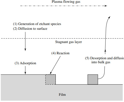
Figure 2.20. Basic steps in dry etching
Plasma etching is a process in which a solid film is removed by a chemical reaction with ground-state or excited-state neutral species. The process is often enhanced or induced by energetic ions generated in a gaseous discharge. Plasma etching proceeds in five steps, as illustrated in Figure 2.20: (1) the etchant species is generated in the plasma, (2) the reactant is then transported by diffusion through a stagnant gas layer to the surface, (3) the reactant is adsorbed on the surface, (4) a chemical reaction (along with physical effects such as ion bombardment) follows to form volatile compounds, and (5) the compounds are desorbed from the surface, diffused into the bulk gas, and pumped out by the vacuum system.
Plasma etching is based on the generation of plasma in a gas at low pressure. Two basic methods are used: physical methods and chemical methods. The former includes sputter etching, and the latter includes pure chemical etching. In physical etching, positive ions bombard the surface at high speed; small amounts of negative ions formed in the plasma cannot reach the wafer surface and therefore play no direct role in plasma etching. In chemical etching, neutral reactive species generated by the plasma interact with the material surface to form volatile products. Chemical and physical etch mechanisms have different characteristics. Chemical etching exhibits a high etch rate, and good selectivity (i.e., the ratio of etch rates for different materials) produces low ion bombardment–induced damage but yields isotropic profiles. Physical etching can yield anisotropic profiles, but it is associated with low etch selectivity and severe bombardment-induced damage. Combinations of chemical and physical etching give anisotropic etch profiles, reasonably good selectivity, and moderate bombardment-induced damage. An example is reactive-ion etching (RIE), which uses a physical method to assist chemical etching or creates reactive ions to participate in chemical etching.
Plasma reactor technology in the IC industry has changed dramatically since the first application of plasma processing to photoresist stripping. A reactor for plasma etching contains a vacuum chamber, pump system, power supply generators, pressure sensors, gas flow control units, and endpoint detector (see Chapter 3). Each etch tool is designed empirically and uses a particular combination of pressure, electrode configuration and type, and source frequency to control the two primary etch mechanisms-chemical and physical. Higher etch rates and tool automation are required for most etchers used in manufacturing.

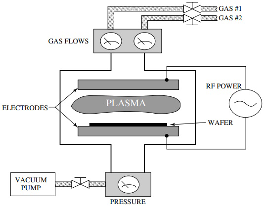
Figure 2.21. Typical reactive-ion etching system
RIE has been extensively used in the microelectronic industry. In a parallel plate diode system (Figure 2.21), a radio frequency (RF), capacitively coupled bottom electrode holds the wafer. This allows the grounded electrode to have a significantly larger area because it is, in fact, the chamber itself. The larger grounded area combined with the lower operating pressure (<500 mTorr) causes the wafers to be subjected to a heavy bombardment of energetic ions from the plasma as a result of the large, negative self-bias at the wafer surface. The etch selectivity of this system is relatively low compared with traditional barrel etch systems because of strong physical sputtering. However, selectivity can be improved by choosing the proper etch chemistry.
This is an excerpt from
Fundamentals of Semiconductor Manufacturing and Process Control by Gary S. May and Costas J. Spanos
A practical guide to semiconductor manufacturing from process control to yield modeling and experimental design. Fundamentals of Semiconductor Manufacturing and Process Control covers all issues involved in manufacturing microelectronic devices and circuits, including fabrication sequences, process control, experimental design, process modeling, yield modeling, and CIM/CAM systems. Readers are introduced to both the theory and practice of all basic manufacturing concepts.
Following an overview of manufacturing and technology, the text explores process monitoring methods, including those that focus on product wafers and those that focus on the equipment used to produce wafers. Next, the text sets forth some fundamentals of statistics and yield modeling, which set the foundation for a detailed discussion of how statistical process control is used to analyze quality and improve yields.
The discussion of statistical experimental design offers readers a powerful approach for systematically varying controllable process conditions and determining their impact on output parameters that measure quality. The authors introduce process modeling concepts, including several advanced process control topics such as run-by-run, supervisory control, and process and equipment diagnosis.
Critical coverage includes the following:
• Combines process control and semiconductor manufacturing
• Unique treatment of system and software technology and management of overall manufacturing systems
• Chapters include case studies, sample problems, and suggested exercises
• Instructor support includes electronic copies of the figures and an instructor's manual
Graduate-level students and industrial practitioners will benefit from the detailed examination of how electronic materials and supplies are converted into finished integrated circuits and electronic products in a high-volume manufacturing environment.
Reader W Boudville says, "For those of you working in a fab, or designing processes to be used in it, May gives a good summary of what is generally known and non-proprietary. He explains the key steps in photolithography, wet and dry etching, the different ways to dope, and deposition processes.
But along with these steps, every fab needs to monitor them for quality control. So we get discussions of how to measure data about a wafer. Like using inteferometry or ellipsometry to measure the thickness of a deposited thin film. Or using a four point probe for capacitance or resistance measurements.
A lot of the text also deals with statistics and how to maximise your device yield. Involves numerous modelling choices and process controls.
Click Here for more information.


