
Optical lithography is so widely used because it has high throughput, good resolution, low cost, and ease of operation. However, due to deep-submicrometer IC process requirements, optical lithography has some limitations that have not yet been solved. Although we can use PSM (Phase-shifting mask) or OPC (Optical proximity correction) to extend its useful lifespan, the complexity of mask production and mask inspection cannot be easily resolved. In addition, the cost of the masks is very high. Therefore, we need to find alternatives to optical lithography to process deep-submicrometer or nanometer ICs.
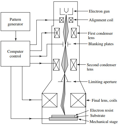
Figure 2.15. E-beam lithography system
Electron-beam (or e-beam) lithography is used primarily to produce photomasks. Relatively few tools are dedicated to direct exposure of the resist by a focused electron beam without a mask. Figure 2.15 shows a schematic of an e-beam lithography system. The electron gun is a device that can generate a beam of electrons with a suitable current density. A tungsten thermionic emission cathode or single-crystal lanthanum hexaboride (LaB6) is used for the electron gun. Condenser lenses are used to focus the electron beam to a spot size 10-25 nm in diameter. Beam blanking plates that turn the electron beam on and off, and beam deflection coils are computer-controlled and operated at MHz or higher rates to direct the focused electron beam to any location in the scan field on the substrate. Because the scan field (typically 1 cm) is much smaller than the substrate diameter, a precision mechanical stage is used to position the substrate to be patterned.
The advantages of electron-beam lithography include the generation of submicrometer resist geometries, highly automated and precisely controlled operation, depth of focus greater than that available from optical lithography, and direct patterning on a semiconductor wafer without using a mask. The disadvantage is that electron-beam lithographic machines have low throughput - approximately 10 wafers per hour at less than 0.25 um resolution. This throughput is adequate for the production of photomasks, for situations that require small numbers of custom circuits, and for design verification. However, for maskless direct writing, the machine must have the highest possible throughput, and therefore, the largest beam diameter possible consistent with the minimum device dimensions.

Figure 2.16. (a) Raster scan and (b) vector scan systems
There are two ways to scan the focused electron beam: raster scan and vector scan. In a raster scan system, resist patterns are written by a beam that moves through a regular mode, vertically oriented, as shown in Figure 2.16a. The beam scans sequentially over every possible location on the mask and is blanked (turned off) where no exposure is required. All patterns on the area to be written must be subdivided into individual addresses, and a given pattern must have a minimum incremental interval that is evenly divisible by the beam address size. In the vector scan system (Figure 2.16b), the beam is directed only to the requested pattern features and jumps from feature to feature, rather than scanning the whole chip, as in raster scan. For many chips, the average exposed region is only 20% of the chip area, which saves time.
Electron resists are polymers. The behavior of an e-beam resist is similar to that of a photoresist; that is, a chemical or physical change is induced in the resist by irradiation. This change allows the resist to be patterned. For a positive electron resist, the polymer-electron interaction causes chemical bonds to be broken (chain scission) to form shorter molecular fragments. As a result, the molecular weight is reduced in the irradiated area, which can be dissolved subsequently in a developer solution that attacks the low=molecular-weight material.
Common positive electron resists include poly(methyl methacrylate) (PMMA) and poly(butene-1 sulfone) (PBS). Positive electron resists can achieve resolution of 0.1 um or better. For a negative electron resist, the irradiation causes radiation-induced polymer linking. The crosslinking creates a complex threedimensional structure with a molecular weight higher than that of the nonirradiated polymer. The nonirradiated resist can be dissolved in a developer solution that does not attack the high-molecular-weight material. Polyglycidylmethacrylate-coethylacrylate (COP) is a common negative electron resist. COP, like most negative photoresists, also swells during development, so the resolution is limited to about 1 um.
While resolution is limited by diffraction of light in optical lithography, in e-beam lithography, the resolution is not impacted by diffraction (because the wavelengths associated with electrons of a few keV and higher energies are less than 0.1 nm), but by electron scattering. When electrons penetrate the resist and underlying substrate, they undergo collisions. These collisions lead to energy losses and path changes. The incident electrons spread out as they travel until either all of their energy is lost or they leave the material because of backscattering.
Because of backscattering, electrons can irradiate regions several micrometers away from the center of the exposure beam. Since the dose of a resist is the sum of the irradiations from all surrounding areas, the electron-beam irradiation at one location will affect the irradiation in neighboring locations. This phenomenon is called the proximity effect. The proximity effect places a limit on the minimum spacings between pattern features. To correct for the proximity effect, patterns are divided into smaller segments. The incident electron dose in each segment is adjusted so that the integrated dose from all its neighboring segments is the correct exposure dose. This approach further decreases the throughput of the electron-beam system, because of the additional computer time required to expose the subdivided resist patterns.
This is an excerpt from

Fundamentals of Semiconductor Manufacturing and Process Control by Gary S. May and Costas J. Spanos
A practical guide to semiconductor manufacturing from process control to yield modeling and experimental design. Fundamentals of Semiconductor Manufacturing and Process Control covers all issues involved in manufacturing microelectronic devices and circuits, including fabrication sequences, process control, experimental design, process modeling, yield modeling, and CIM/CAM systems. Readers are introduced to both the theory and practice of all basic manufacturing concepts.
Following an overview of manufacturing and technology, the text explores process monitoring methods, including those that focus on product wafers and those that focus on the equipment used to produce wafers. Next, the text sets forth some fundamentals of statistics and yield modeling, which set the foundation for a detailed discussion of how statistical process control is used to analyze quality and improve yields.
The discussion of statistical experimental design offers readers a powerful approach for systematically varying controllable process conditions and determining their impact on output parameters that measure quality. The authors introduce process modeling concepts, including several advanced process control topics such as run-by-run, supervisory control, and process and equipment diagnosis.
Critical coverage includes the following:
• Combines process control and semiconductor manufacturing
• Unique treatment of system and software technology and management of overall manufacturing systems
• Chapters include case studies, sample problems, and suggested exercises
• Instructor support includes electronic copies of the figures and an instructor's manual
Graduate-level students and industrial practitioners will benefit from the detailed examination of how electronic materials and supplies are converted into finished integrated circuits and electronic products in a high-volume manufacturing environment.
Reader W Boudville says, "For those of you working in a fab, or designing processes to be used in it, May gives a good summary of what is generally known and non-proprietary. He explains the key steps in photolithography, wet and dry etching, the different ways to dope, and deposition processes.
But along with these steps, every fab needs to monitor them for quality control. So we get discussions of how to measure data about a wafer. Like using inteferometry or ellipsometry to measure the thickness of a deposited thin film. Or using a four point probe for capacitance or resistance measurements.
A lot of the text also deals with statistics and how to maximise your device yield. Involves numerous modelling choices and process controls.
Click Here for more information.
