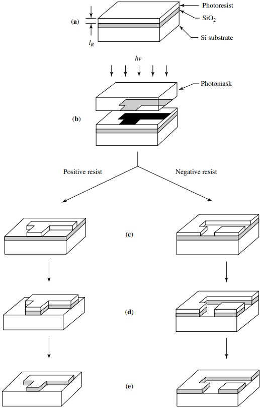
 Figure 2.14. Photolithographic pattern transfer process: (a) photoresist application;
(b) exposure; (c) development; (d) etching; (e) resist stripping
Figure 2.14 illustrates the steps to transfer IC patterns from a mask to a silicon wafer that has an insulating SiO2 layer formed on its surface. The wafer is placed in a cleanroom, which typically is illuminated with yellow light (since photoresists are not sensitive to wavelengths greater than 0.5 um). To ensure satisfactory adhesion of the resist, adhesion promoter is then applied. The most common adhesion promoter for silicon ICs is hexamethylene-disiloxane (HMDS).
After the application of this adhesion layer, the wafer is held on a vacuum spindle, and liquidous resist is applied to the center of wafer. The wafer is then rapidly accelerated up to a constant rotational speed, which is maintained for about 30 s. Spin speed is generally in the range of 1000-10,000 rpm [revolutions per minute (r/min)] to coat a uniform film about 0.5-1 um thick, as shown in Figure 2.14a. The thickness of photoresist is correlated with its viscosity.
After spinning, the wafer is "soft-baked" (typically at 90-120o C for 60-120 s) to remove solvent from the photoresist and to increase resist adhesion to the wafer. The wafer is aligned with respect to the mask in an optical lithographic system, and the resist is exposed to ultraviolet light, as shown in Figure 2.14b. If a positive photoresist is used, the exposed resist is dissolved in the developer, as shown on the left side of Figure 2.14c. Photoresist development is usually done by flooding the wafer with the developer solution.
The wafer is then rinsed and dried. After development, "postbaking" at approximately 100-180o C may be required to increase the adhesion of the resist to the substrate. The wafer is then put in an ambient that etches the exposed insulation layer but does not attack the resist, as shown in Figure 2.14d. Finally, the resist is stripped (using solvents or plasma oxidation), leaving behind an insulator image that is the same as the opaque image on the mask (left side of Figure 2.14e). For negative photoresist, the procedures described are also applicable, except that the unexposed areas are removed. The final insulator image (right side of Figure 2.14e) is the reverse of the opaque image on the mask.
The insulator image can be used as a mask for subsequent processing. For example, ion implantation can be done to dope the exposed semiconductor region, but not the area covered by the insulator. The dopant pattern is a duplicate of the design pattern on the photomask for a negative photoresist or is its complementary pattern for a positive photoresist. The complete circuit is fabricated by aligning the next mask in the sequence to the previous pattern and repeating the lithographic transfer process.
This is an excerpt from
Fundamentals of Semiconductor Manufacturing and Process Control by Gary S. May and Costas J. Spanos
A practical guide to semiconductor manufacturing from process control to yield modeling and experimental design. Fundamentals of Semiconductor Manufacturing and Process Control covers all issues involved in manufacturing microelectronic devices and circuits, including fabrication sequences, process control, experimental design, process modeling, yield modeling, and CIM/CAM systems. Readers are introduced to both the theory and practice of all basic manufacturing concepts.
Following an overview of manufacturing and technology, the text explores process monitoring methods, including those that focus on product wafers and those that focus on the equipment used to produce wafers. Next, the text sets forth some fundamentals of statistics and yield modeling, which set the foundation for a detailed discussion of how statistical process control is used to analyze quality and improve yields.
The discussion of statistical experimental design offers readers a powerful approach for systematically varying controllable process conditions and determining their impact on output parameters that measure quality. The authors introduce process modeling concepts, including several advanced process control topics such as run-by-run, supervisory control, and process and equipment diagnosis.
Critical coverage includes the following:
• Combines process control and semiconductor manufacturing
• Unique treatment of system and software technology and management of overall manufacturing systems
• Chapters include case studies, sample problems, and suggested exercises
• Instructor support includes electronic copies of the figures and an instructor's manual
Graduate-level students and industrial practitioners will benefit from the detailed examination of how electronic materials and supplies are converted into finished integrated circuits and electronic products in a high-volume manufacturing environment.
Reader W Boudville says, "For those of you working in a fab, or designing processes to be used in it, May gives a good summary of what is generally known and non-proprietary. He explains the key steps in photolithography, wet and dry etching, the different ways to dope, and deposition processes.
But along with these steps, every fab needs to monitor them for quality control. So we get discussions of how to measure data about a wafer. Like using inteferometry or ellipsometry to measure the thickness of a deposited thin film. Or using a four point probe for capacitance or resistance measurements.
A lot of the text also deals with statistics and how to maximise your device yield. Involves numerous modelling choices and process controls.
Click Here for more information.


