
Photoresist is a radiation-sensitive compound that can be classified as positive or negative, depending on how they respond to radiation. For positive resists, the exposed regions become more soluble and thus more easily removed in the development process. The result is that the patterns formed in the positive resist are the same as those on the mask. Positive photoresists consist of three components: a photosensitive compound, a base resin, and an organic solvent. Prior to exposure, the photosensitive compound is insoluble in the developer solution. After exposure, the photosensitive compound absorbs radiation in the exposed pattern areas, changes its chemical structure, and becomes soluble in the developer solution. After development, the exposed areas are removed.
With negative resists, exposed regions become less soluble, and the patterns formed in the negative resist are the reverse of the mask patterns. Negative photoresists are polymers combined with a photosensitive compound. After exposure, the photosensitive compound absorbs the optical energy and converts it into chemical energy to initiate a polymer crosslinking reaction. This reaction causes crosslinking of the polymer molecules. The crosslinked polymer has a higher molecular weight and becomes insoluble in the developer solution. After development, the unexposed areas are removed. One major drawback of a negative photoresist is that in the development process, the whole resist mass swells by absorbing developer solvent. This swelling action limits the resolution of negative photoresists..
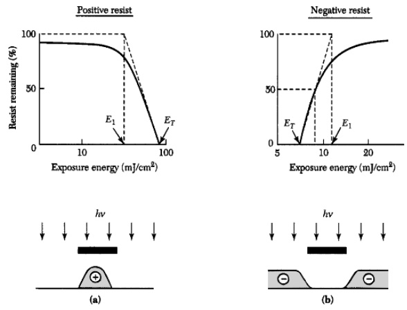
Figure 2.13. Exposure response curve and cross section of resist image after development
for (a) positive photoresist and (b) negative photoresist
Figure 2.13a shows a typical exposure response curve and image cross section for a positive resist. The response curve describes the percentage of resist remaining after exposure and development versus the exposure energy. As the exposure energy increases the solubility gradually increases until at a threshold energy ET , the resist becomes completely soluble. The sensitivity of a positive resist is defined as the energy required to produce complete solubility in the exposed region. Thus, ET corresponds to the sensitivity. In addition to ET , a parameter γ, the contrast ratio, is defined to characterize the resist.
(equation 2.19)
where E1 is the energy obtained by drawing the tangent at ET to reach 100% resist thickness, as shown in Figure 2.13a. A larger γ implies a higher solubility of the resist with an incremental increase of exposure energy and results in sharper images.
The image cross section in Figure 2.13a illustrates the relationship between the edges of a photomask image and the corresponding edges of the resist images after development. The edges of the resist image are generally not at the vertically projected positions of the mask edges because of diffraction. The edge of the resist image corresponds to the position where the total absorbed optical energy equals the threshold energy ET.
Figure 2.13b shows the exposure response curve and image cross section for a negative resist. The negative resist remains completely soluble in the developer solution for exposure energies lower than ET . Above ET , more of the resist film remains after development. At exposure energies twice the threshold energy, the resist film becomes essentially insoluble in the developer. The sensitivity of a negative resist is defined as the energy required to retain 50% of the original resist film thickness in the exposed region. The parameter γ is defined similarly to γ in Eq. (2.19), except that E1 and ET are interchanged. The image cross section for the negative resist (Figure 2.13b) is also influenced by the diffraction effect.
This is an excerpt from

Fundamentals of Semiconductor Manufacturing and Process Control by Gary S. May and Costas J. Spanos
A practical guide to semiconductor manufacturing from process control to yield modeling and experimental design. Fundamentals of Semiconductor Manufacturing and Process Control covers all issues involved in manufacturing microelectronic devices and circuits, including fabrication sequences, process control, experimental design, process modeling, yield modeling, and CIM/CAM systems. Readers are introduced to both the theory and practice of all basic manufacturing concepts.
Following an overview of manufacturing and technology, the text explores process monitoring methods, including those that focus on product wafers and those that focus on the equipment used to produce wafers. Next, the text sets forth some fundamentals of statistics and yield modeling, which set the foundation for a detailed discussion of how statistical process control is used to analyze quality and improve yields.
The discussion of statistical experimental design offers readers a powerful approach for systematically varying controllable process conditions and determining their impact on output parameters that measure quality. The authors introduce process modeling concepts, including several advanced process control topics such as run-by-run, supervisory control, and process and equipment diagnosis.
Critical coverage includes the following:
• Combines process control and semiconductor manufacturing
• Unique treatment of system and software technology and management of overall manufacturing systems
• Chapters include case studies, sample problems, and suggested exercises
• Instructor support includes electronic copies of the figures and an instructor's manual
Graduate-level students and industrial practitioners will benefit from the detailed examination of how electronic materials and supplies are converted into finished integrated circuits and electronic products in a high-volume manufacturing environment.
Reader W Boudville says, "For those of you working in a fab, or designing processes to be used in it, May gives a good summary of what is generally known and non-proprietary. He explains the key steps in photolithography, wet and dry etching, the different ways to dope, and deposition processes.
But along with these steps, every fab needs to monitor them for quality control. So we get discussions of how to measure data about a wafer. Like using inteferometry or ellipsometry to measure the thickness of a deposited thin film. Or using a four point probe for capacitance or resistance measurements.
A lot of the text also deals with statistics and how to maximise your device yield. Involves numerous modelling choices and process controls.
Click Here for more information.
