Masks used for semiconductor manufacturing are usually reduction reticles. The first step in maskmaking is to use a computer-aided design (CAD) system in which designers can completely describe the circuit patterns electrically. The digital data produced by the CAD system then drive a pattern generator, which is an electron-beam lithographic system that transfers the patterns directly to electron-sensitized mask. The mask consists of a fusedsilica substrate covered with a chrominum layer.
The circuit pattern is first transferred to the electron-sensitized layer (electron resist), which is transferred once more into the underlying chrominum layer for the finished mask. The patterns on a mask represent one level of an IC design. The composite layout is broken into mask levels that correspond to the manufacturing process sequence, such as the isolation region on one level, the gate region on another, and so on. Typically, 15-20 different mask levels are required for a complete IC process cycle.

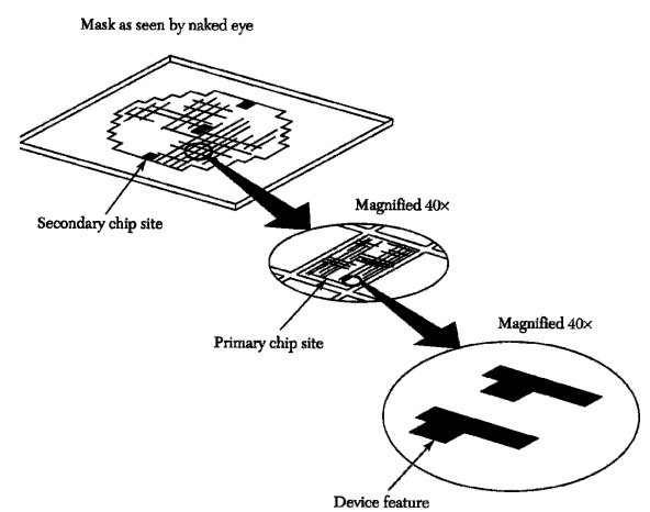
Figure 2.12. A typical IC photomask
The standard-size mask substrate is a fused-silica plate 15 x 15 cm square, 0.6 cm thick. This size is needed to accommodate the lens field sizes for 4 : 1 or 5 : 1 optical exposure tools, whereas the thickness is required to minimize pattern placement errors due to substrate distortion. The fused-silica plate is needed for its low coefficient of thermal expansion, its high transmission at shorter wavelengths, and its mechanical strength. Figure 2.12 shows a mask on which patterns of geometric shapes have been formed. A few secondary-chip sites, used for process evaluation, are also included in the mask.
One of the major concerns about masks is the defect density. Mask defects can be introduced during the manufacture of the mask or during subsequent lithographic processes. Even a small mask defect density has a profound effect on the final IC yield. Yield is defined as the ratio of good chips per wafer to the total number of chips per wafer. Inspection and cleaning of masks are important to achieve high yields on large chips. An ultraclean processing area is mandatory for photolithographic processing.
This is an excerpt from
Fundamentals of Semiconductor Manufacturing and Process Control by Gary S. May and Costas J. Spanos
A practical guide to semiconductor manufacturing from process control to yield modeling and experimental design. Fundamentals of Semiconductor Manufacturing and Process Control covers all issues involved in manufacturing microelectronic devices and circuits, including fabrication sequences, process control, experimental design, process modeling, yield modeling, and CIM/CAM systems. Readers are introduced to both the theory and practice of all basic manufacturing concepts.
Following an overview of manufacturing and technology, the text explores process monitoring methods, including those that focus on product wafers and those that focus on the equipment used to produce wafers. Next, the text sets forth some fundamentals of statistics and yield modeling, which set the foundation for a detailed discussion of how statistical process control is used to analyze quality and improve yields.
The discussion of statistical experimental design offers readers a powerful approach for systematically varying controllable process conditions and determining their impact on output parameters that measure quality. The authors introduce process modeling concepts, including several advanced process control topics such as run-by-run, supervisory control, and process and equipment diagnosis.
Critical coverage includes the following:
• Combines process control and semiconductor manufacturing
• Unique treatment of system and software technology and management of overall manufacturing systems
• Chapters include case studies, sample problems, and suggested exercises
• Instructor support includes electronic copies of the figures and an instructor's manual
Graduate-level students and industrial practitioners will benefit from the detailed examination of how electronic materials and supplies are converted into finished integrated circuits and electronic products in a high-volume manufacturing environment.
Reader W Boudville says, "For those of you working in a fab, or designing processes to be used in it, May gives a good summary of what is generally known and non-proprietary. He explains the key steps in photolithography, wet and dry etching, the different ways to dope, and deposition processes.
But along with these steps, every fab needs to monitor them for quality control. So we get discussions of how to measure data about a wafer. Like using inteferometry or ellipsometry to measure the thickness of a deposited thin film. Or using a four point probe for capacitance or resistance measurements.
A lot of the text also deals with statistics and how to maximise your device yield. Involves numerous modelling choices and process controls.
Click Here for more information.


