Photolithography is the process of transferring patterns of geometric shapes on a mask to a thin layer of photosensitive material (called photoresist) covering the surface of a semiconductor wafer. These patterns define the various regions in an integrated circuit, such as the implantation regions, the contact windows, and the bonding pad areas. The resist patterns defined by the lithographic process are not permanent elements of the final device, but only replicas of circuit features. To produce circuit features, these resist patterns must be transferred once more into the underlying layers of the device. Pattern transfer is accomplished by an etching process that selectively removes unmasked portions of a layer.

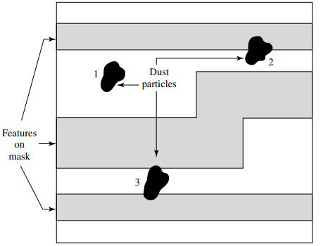
Figure 2.8. Various ways in which particles can interfere with photomask patterns
Photolithography requires a clean processing room. The need for a cleanroom arises because dust particles in the air can settle on semiconductor wafers or lithographic masks and cause defects that result in circuit failure. For example, a dust particle on a semiconductor surface can disrupt the growth of an epitaxial film, causing the formation of dislocations. A dust particle incorporated into a gate oxide can result in enhanced conductivity and cause device failure due to low breakdown voltage. The situation is even more critical in photolithography.
When dust particles adhere to the surface of a photomask, they behave as opaque patterns on the mask, and these patterns will be transferred to the underlying layer along with the circuit patterns on the mask. Figure 2.8 shows three dust particles on a photomask. Particle 1 may result in the formation of a pinhole in the underlying layer. Particle 2 is located near a pattern edge and may cause a constriction of current flow in a metal runner. Particle 3 can lead to a short circuit between the two conducting regions and render the circuit useless.
In a cleanroom, the total number of dust particles per unit volume must be tightly controlled along with the temperature and humidity. There are two systems to define the classes of cleanroom. For the English system, the numerical designation of the class is taken from the maximum allowable number of particles 0.5 µm and larger per cubic foot of air. For the metric system, the class is taken from the logarithm (base 10) of the maximum allowable number of particles 0.5 µm and larger, per cubic meter. For example, a class 100 cleanroom (English system) has a dust count of 100 particles/ft3 with particle diameters of 0.5 µm and larger, whereas a class M 3.5 cleanroom (metric system) has a dust count of 103.5 or about 3500 particles/m3 with particle diameters of 0.5 µm or larger.
Since the number of dust particles increases as particle size decreases, more stringent control of the cleanroom environment is required as the minimum feature lengths of ICs are reduced. For most IC fabrication areas, a class 100 cleanroom is required; that is, the dust count must be about four orders of magnitude lower than that of ordinary room air. However, for photolithography, a class 10 cleanroom or one with a lower dust count is required.
Exposure Tools
The pattern transfer process is accomplished by using a lithographic exposure tool. The performance of an exposure tool is determined by resolution, registration, and throughput. Resolution is the minimum feature dimension that can be transferred with high fidelity to a resist film on a semiconductor wafer. Registration is a measure of how accurately patterns on successive masks can be aligned (or overlaid with respect to previously defined patterns on the wafer. Throughput is the number of wafers that can be exposed per unit time for a given mask level.
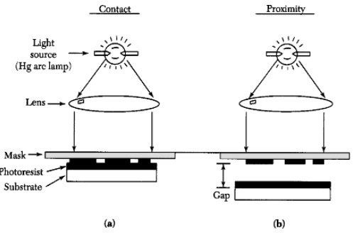
There are two primary optical exposure methods: shadow printing and projection printing. Shadow printing may have the mask and wafer in direct contact with one another (as in contact printing), or in close proximity (as in proximity printing). Figure 2.9a shows a basic setup for contact printing where a resist-coated wafer is brought into physical contact with a mask, and the resist is exposed by a nearly collimated beam of ultraviolet light through the back of the mask for a fixed time. The intimate contact between the resist and mask provides a resolution of ~1 µm. However, contact printing suffers from one major drawback - a dust particle on the wafer can be embedded into the mask when the mask makes contact with the wafer. The embedded particle causes permanent damage to the mask and results in defects in the wafer with each succeeding exposure.
To minimize mask damage, the proximity exposure method is used. Figure 2.9b shows the basic setup, which is similar to contact printing except that there is a small gap (10-50 um) between the wafer and the mask during exposure. The small gap, however, results in optical diffraction at feature edges on the photomask; that is, when light passes by the edges of an opaque mask feature, fringes are formed and some light penetrates into the shadow region. As a result, resolution is degraded to the 2-5-um range.

Figure 2.9. Optical shadow printing techniques: (a) contact printing; (b) proximity printing
In shadow printing, the minimum linewidth, or critical dimension (CD), that can be printed is approximately.
CD ≈
(equation 2.15)
where λ is the wavelength of the exposure radiation and g is the gap between the mask and the wafer and includes the thickness of the resist. For λ = 0.4 um and g = 50 um, the CD is 4.5 um. If we reduce λ to 0.25 um (a wavelength range of 0.2-0.3 um is in the deep-UV spectral region) and g to 15 um, the CD becomes 2 um. Thus, there is an advantage in reducing both λ and g. However, for a given distance g, any dust particle with a diameter larger than g potentially can cause mask damage.
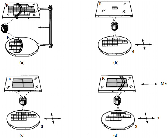
To avoid the mask damage problem associated with shadow printing, projection printing tools have been developed to project an image of the mask patterns onto a resist-coated wafer many centimeters away from the mask. To increase resolution, only a small portion of the mask is exposed at a time. The small image area is scanned or stepped over the wafer to cover the entire wafer surface. Figure 2.10a shows a 1 : 1 wafer scan projection system. A narrow, arc-shaped image field ~1 mm in width serially transfers the slit image of the mask onto the wafer. The image size on the wafer is the same as that on the mask.
The small image field can also be stepped over the surface of the wafer by twodimensional translations of the wafer only, whereas the mark remains stationary. After the exposure of one chip site, the wafer is moved to the next chip site and the process is repeated. Figures 2.10b and 2.10c show the partitioning of the wafer image by step-and-repeat projection with a ratio of 1 : 1 or at a demagnification ratio M : 1 (e.g., 10 : 1 for a 10 times reduction on the wafer), respectively. The 1 : 1 optical systems are easier to design and fabricate than a 10 : 1 or a 5 : 1 reduction system, but it is much more difficult to produce defect-free masks at 1 : 1 than it is at a 10 : 1 or a 5 : 1 demagnification ratio.

Figure 2.10. Image partitioning techniques for projection printing: (a) annual field wafer scan;
(b) 1 : 1 step-and-repeat; (c) M : 1 step-and-repeat; and (d) M : 1 step-and-scan
Reduction projection lithography can also print larger wafers without redesigning the stepper lens, as long as the field size (i.e., the exposure area onto the wafer) of the lens is large enough to contain one or more ICs. When the chip size exceeds the field size of the lens, further partitioning of the image on the reticle is necessary. In Figure 2.10d, the image field on the reticle can be a narrow, arc shape for M : 1 step-and-scan projection lithography. For the step-and-scan system, we have two-dimensional translations of the wafer with speed v, and one-dimensional translation of the mask with M times that of the wafer speed.
The resolution of a projection system is given by
Im = k1
(equation 2.16)
where k1 is a process-dependent factor and NA is the numerical aperture, which is given by
NA = sin θ(equation 2.17)

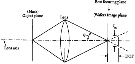
Figure 2.11. Illustration of DoF
where is the index of refraction in the image medium (usually air, where = 1) and θ is the half-angle of the cone of light converging to a point image at the wafer, as shown in Figure 2.11. Also shown in the figure is the depth of focus (DoF), which can be expressed as
(equation 2.18)
Equation (2.16) indicates that resolution can be improved (i.e., smaller lm) by either reducing the wavelength, increasing NA, or both. However, Eq. (2.18) indicates that the DoF degrades much more rapidly by increasing NA than by decreasing λ. This explains the trend toward shorter-wavelength sources in optical lithography.
This is an excerpt from
Fundamentals of Semiconductor Manufacturing and Process Control by Gary S. May and Costas J. Spanos
A practical guide to semiconductor manufacturing from process control to yield modeling and experimental design. Fundamentals of Semiconductor Manufacturing and Process Control covers all issues involved in manufacturing microelectronic devices and circuits, including fabrication sequences, process control, experimental design, process modeling, yield modeling, and CIM/CAM systems. Readers are introduced to both the theory and practice of all basic manufacturing concepts.
Following an overview of manufacturing and technology, the text explores process monitoring methods, including those that focus on product wafers and those that focus on the equipment used to produce wafers. Next, the text sets forth some fundamentals of statistics and yield modeling, which set the foundation for a detailed discussion of how statistical process control is used to analyze quality and improve yields.
The discussion of statistical experimental design offers readers a powerful approach for systematically varying controllable process conditions and determining their impact on output parameters that measure quality. The authors introduce process modeling concepts, including several advanced process control topics such as run-by-run, supervisory control, and process and equipment diagnosis.
Critical coverage includes the following:
• Combines process control and semiconductor manufacturing
• Unique treatment of system and software technology and management of overall manufacturing systems
• Chapters include case studies, sample problems, and suggested exercises
• Instructor support includes electronic copies of the figures and an instructor's manual
Graduate-level students and industrial practitioners will benefit from the detailed examination of how electronic materials and supplies are converted into finished integrated circuits and electronic products in a high-volume manufacturing environment.
Reader W Boudville says, "For those of you working in a fab, or designing processes to be used in it, May gives a good summary of what is generally known and non-proprietary. He explains the key steps in photolithography, wet and dry etching, the different ways to dope, and deposition processes.
But along with these steps, every fab needs to monitor them for quality control. So we get discussions of how to measure data about a wafer. Like using inteferometry or ellipsometry to measure the thickness of a deposited thin film. Or using a four point probe for capacitance or resistance measurements.
A lot of the text also deals with statistics and how to maximise your device yield. Involves numerous modelling choices and process controls.
Click Here for more information.


