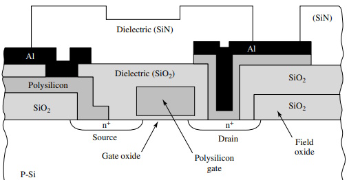
Many different kinds of thin films are used to fabricate discrete devices and integrated circuits, including thermal oxides, dielectric layers, polycrystalline silicon, and metal films. For example, a silicon n-channel MOSFET (Figure 2.1) uses all four groups of films.

Figure 2.1. Cross section of a MOSFET
An important oxide layer is the gate oxide, under which a conducting channel can be formed between the source and the drain. A related layer is the field oxide, which provides isolation from other devices. Both gate and field oxides generally are grown by a thermal oxidation process because only thermal oxidation can provide the highest-quality oxides having the lowest interface trap densities.

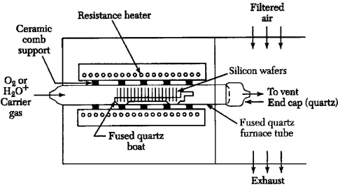
Figure 2.2. Schematic of an oxidation furnace
Semiconductors can be oxidized by various methods, including thermal oxidation, electrochemical anodization, and plasma-enhanced chemical vapor deposition. Among these, thermal oxidation is the most important for silicon devices. It is a key process in modern silicon IC technology. The basic thermal oxidation apparatus (shown in Figure 2.2) consists of a resistance-heated furnace, a cylindrical fused-quartz tube containing the silicon wafers held vertically in a slotted quartz boat, and a source of either pure dry oxygen or pure water vapor. Oxidation temperature is generally in the range of 900–1200 degrees C, and the typical gas flowrate is about 1 L/min.
The oxidation system uses microprocessors to regulate the gas flow sequence, to control the automatic insertion and removal of silicon wafers, to ramp the temperature up (i.e., to increase the furnace temperature linearly) from a low temperature to the oxidation temperature, to maintain the oxidation temperature to within ±1 degree C, and to ramp the temperature down when oxidation is completed.
This is an excerpt from
Fundamentals of Semiconductor Manufacturing and Process Control by Gary S. May and Costas J. Spanos
A practical guide to semiconductor manufacturing from process control to yield modeling and experimental design. Fundamentals of Semiconductor Manufacturing and Process Control covers all issues involved in manufacturing microelectronic devices and circuits, including fabrication sequences, process control, experimental design, process modeling, yield modeling, and CIM/CAM systems. Readers are introduced to both the theory and practice of all basic manufacturing concepts.
Following an overview of manufacturing and technology, the text explores process monitoring methods, including those that focus on product wafers and those that focus on the equipment used to produce wafers. Next, the text sets forth some fundamentals of statistics and yield modeling, which set the foundation for a detailed discussion of how statistical process control is used to analyze quality and improve yields.
The discussion of statistical experimental design offers readers a powerful approach for systematically varying controllable process conditions and determining their impact on output parameters that measure quality. The authors introduce process modeling concepts, including several advanced process control topics such as run-by-run, supervisory control, and process and equipment diagnosis.
Critical coverage includes the following:
• Combines process control and semiconductor manufacturing
• Unique treatment of system and software technology and management of overall manufacturing systems
• Chapters include case studies, sample problems, and suggested exercises
• Instructor support includes electronic copies of the figures and an instructor's manual
Graduate-level students and industrial practitioners will benefit from the detailed examination of how electronic materials and supplies are converted into finished integrated circuits and electronic products in a high-volume manufacturing environment.
Reader W Boudville says, "For those of you working in a fab, or designing processes to be used in it, May gives a good summary of what is generally known and non-proprietary. He explains the key steps in photolithography, wet and dry etching, the different ways to dope, and deposition processes.
But along with these steps, every fab needs to monitor them for quality control. So we get discussions of how to measure data about a wafer. Like using inteferometry or ellipsometry to measure the thickness of a deposited thin film. Or using a four point probe for capacitance or resistance measurements.
A lot of the text also deals with statistics and how to maximise your device yield. Involves numerous modelling choices and process controls.
Click Here for more information.

Learn more at amazon.com

