The semiconductor manufacturing process can be defined at various levels of abstraction. For example, each process step has inputs, outputs, and specifications. Each step can also be modeled, either physically, empirically, or both. At a higher level of abstraction, multiple process steps are linked together to form a process sequence. Between some of these links are inspection points, which merely produce information without changing the product. The flow and utilization of information occurs at another level of abstraction, which consists of various control loops. Finally, the organization of the process belongs to yet another level of abstraction, where the objective is to maximize the efficiency of product flow while reducing variability.
Unit Processes
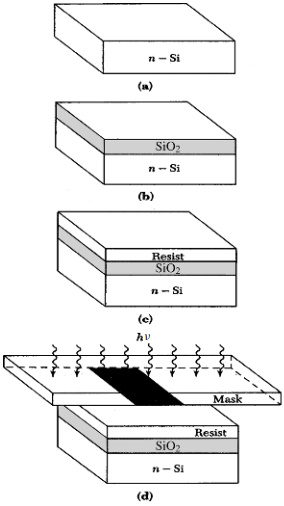
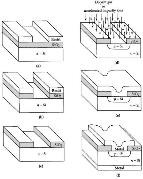
It is difficult to discuss unit process steps outside the context of a process flow. Figures 1.4 and 1.5 show the major unit processes used in a simple process flow. These steps include oxidation, photolithography, etching, ion implantation, and metallization. We describe these steps briefly in this section via a simple sequence used to fabricate a p-n junction.

Figure 1.4. (a) A bare n-type silicon wafer; (b) an oxidized silicon wafer; (c)
application of photoresist; (d) resist exposure through a mask.

Figure 1.5. (a) Wafer after development; (b) wafer after SiO2 removal; (c) result after
photolithography; (d) formation of a p-n junction using diffusion or implantation;
(e) wafer after metallization; (f) final product.
The development of a high-quality silicon dioxide (SiO2) has helped to establish the dominance of silicon in the production of commercial ICs. Generally, SiO2 functions as an insulator in a number of device structures or as a barrier to diffusion or implantation during device fabrication. In the fabrication of a p-n junction (Figure 1.4), the SiO2 film is used to define the junction area. There are two SiO2 growth methods, dry and wet oxidation, depending on whether dry oxygen or water vapor is used. Dry oxidation is usually used to form thin oxides in a device structure because of its good Si-SiO2 interface characteristics, whereas wet oxidation is used for thicker layers because of its higher growth rate. Figure 1.4a shows a section of a bare wafer ready for oxidation. After the oxidation process, a SiO2 layer is formed all over the wafer surface. For simplicity, Figure 1.4b shows only the upper surface of an oxidized wafer.
Photolithography is used to define the geometry of the p-n junction. After the formation of SiO2, the wafer is coated with an ultraviolet (UV) light-sensitive material called photoresist, which is spun onto the wafer surface. Afterward (Figure 1.4c), the wafer is baked to drive the solvent out of the resist and to harden the resist for improved adhesion. Figure 1.4d shows the next step, which is to expose the wafer through a patterned mask using an UV light source. The exposed region of the photoresist-coated wafer undergoes a chemical reaction. The exposed area becomes polymerized and difficult to remove in an etchant. The polymerized region remains when the wafer is placed in a developer, whereas the unexposed region dissolves away.
Figure 1.5a shows the wafer after the development. The wafer is again baked to enhance the adhesion and improve the resistance to the subsequent etching process. Then, an etch using hydrofluoric acid (HF) removes the unprotected SiO2 surface (Figure 1.5b). Last, the resist is stripped away by a chemical solution or an oxygen plasma. Figure 1.5c shows the final result of a region without oxide (a window) after the lithography process. The wafer is now ready for forming the p-n junction by a diffusion or ion implantation process.
In diffusion, the wafer surface not protected by the oxide is exposed to a source with a high concentration of an opposite-type impurity. The impurity moves into the semiconductor crystal by solid-state diffusion. In ion implantation, the intended impurity is introduced into the wafer by accelerating the impurity ions to a high energy level and then implanting the ions in the semiconductor. The SiO2 layer serves as barrier to impurity diffusion or ion implantation. After diffusion or implantation, the p-n junction is formed (Figure 1.5d).
After diffusion or ion implantation, a metallization process is used to form ohmic contacts and interconnections (Figure 1.5e). Metal films can be formed by physical vapor deposition or chemical vapor deposition. The photolithography process is again used to define the front contact, which is shown in Figure 1.5f. A similar metallization step is performed on the back contact without using a photolithography process.
This is an excerpt from
Fundamentals of Semiconductor Manufacturing and Process Control by Gary S. May and Costas J. Spanos
A practical guide to semiconductor manufacturing from process control to yield modeling and experimental design. Fundamentals of Semiconductor Manufacturing and Process Control covers all issues involved in manufacturing microelectronic devices and circuits, including fabrication sequences, process control, experimental design, process modeling, yield modeling, and CIM/CAM systems. Readers are introduced to both the theory and practice of all basic manufacturing concepts.
Following an overview of manufacturing and technology, the text explores process monitoring methods, including those that focus on product wafers and those that focus on the equipment used to produce wafers. Next, the text sets forth some fundamentals of statistics and yield modeling, which set the foundation for a detailed discussion of how statistical process control is used to analyze quality and improve yields.
The discussion of statistical experimental design offers readers a powerful approach for systematically varying controllable process conditions and determining their impact on output parameters that measure quality. The authors introduce process modeling concepts, including several advanced process control topics such as run-by-run, supervisory control, and process and equipment diagnosis.
Critical coverage includes the following:
• Combines process control and semiconductor manufacturing
• Unique treatment of system and software technology and management of overall manufacturing systems
• Chapters include case studies, sample problems, and suggested exercises
• Instructor support includes electronic copies of the figures and an instructor's manual
Graduate-level students and industrial practitioners will benefit from the detailed examination of how electronic materials and supplies are converted into finished integrated circuits and electronic products in a high-volume manufacturing environment.
Reader W Boudville says, "For those of you working in a fab, or designing processes to be used in it, May gives a good summary of what is generally known and non-proprietary. He explains the key steps in photolithography, wet and dry etching, the different ways to dope, and deposition processes.
But along with these steps, every fab needs to monitor them for quality control. So we get discussions of how to measure data about a wafer. Like using inteferometry or ellipsometry to measure the thickness of a deposited thin film. Or using a four point probe for capacitance or resistance measurements.
A lot of the text also deals with statistics and how to maximise your device yield. Involves numerous modelling choices and process controls.
Click Here for more information.


