A zener diode is similar to a standard diode consisting of a semiconductor PN junction. When biased with the anode positive with respect to the cathode, it behaves just like a normal diode, allowing current to flow in the forward direction with a voltage drop of 0.3 to 0.7 volts, and blocking current flow in the reverse direction.

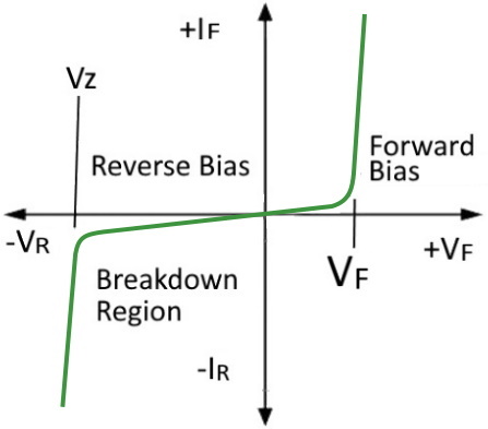
V-I curve of zener diode
And just like a normal diode, at a certain reverse voltage the junction will break down and allow current to flow in reverse. The difference is that in a zener diode the semiconductor is more heavily doped than a normal diode, and this allows it to operate in the reverse-bias break down mode.
The reverse-bias break down voltage, in this case called the "zener" voltage, is set during the manufacturing process by controlling the doping level. The manufacturing process can produce diodes with zener voltages between about 2 and 200 volts. Operating a zener diode in the breakdown region does not damage it, as long as the maximum power dissipation rating of the zener isnot exceed.

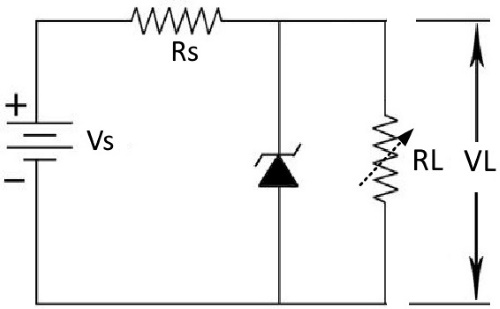
The schematic above shows the zener diode symbol
This ability of the zener diode to maintian a constant reverse voltage can be used to regulate a voltage against supply or load variations. The fact that the voltage across the diode in the breakdown region is almost constant turns out to be an useful characteristic of the zener diode in the design of simple voltage regulator circuits.

