A JFET can have any of several different forms. They all work the same way: the current varies because of the effects of an electric field within the device.
The workings inside a JFET can be likened to the control of water flow through a garden hose. Electrons or holes pass from the source (S) electrode to the drain (D). This results in a drain current, ID, that is generally the same as the source current, IS. This is analogous to the fact that the water comes out of a garden hose at the same rate it goes in (assuming that there aren't any leaks in the hose).
The rate of flow of charge carriers - that is, the current - depends on the voltage at a regulating electrode called the gate (G). Fluctuations in gate voltage, EG, cause changes in the current through the channel, IS or ID. Small fluctuations in the control voltage EG can cause large variations in the flow of charge carriers through the JFET. This translates into voltage amplification in electronic circuits.
N-channel versus P-channel
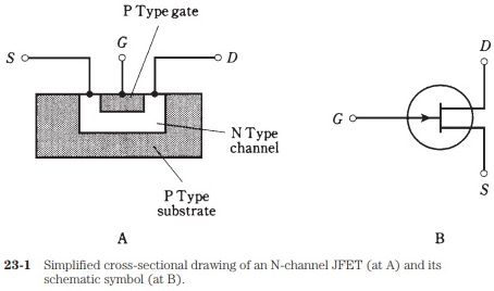
A simplified drawing of an N-channel JFET, and its schematic symbol, are shown in Fig. 23-1. The N-type material forms the channel, or the path for charge carriers. In the N-channel device, the majority carriers are electrons. The source is at one end of the channel, and the drain is at the other. You can think of electrons as being "injected" into the source and "collected" from the drain as they pass through the channel. The drain is positive with respect to the source.

In an N-channel device, the gate consists of P-type material. Another, larger section P-type material, called the substrate, forms a boundary on the side of the channel opposite the gate. The JFET is formed in the substrate during manufacture by a process known as diffusion.
The voltage on the gate produces an electric field that interferes with the flow of charge carriers through the channel. The more negative EG becomes, the more the electric field chokes off the current though the channel, and the smaller ID becomes.
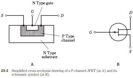
A P-channel JFET (Fig. 23-2) has a channel of P-type semiconductor. The majority charge carriers are holes. The drain is negative with respect to the source. In a sense, holes are "injected" into the source and are "collected" from the drain. The gate and the substrate are of N-type material.
In the P-channel JFET, the more positive EG gets, the more the electric field chokes off the current through the channel, and the smaller ID becomes.
You can recognize the N-channel device by the arrow pointing inward at the gate, and the P-channel JFET by the arrow pointing outward. Also, you can tell which is which (sometimes arrows are not included in schematic diagrams) by the power-supply polarity. A positive drain indicates an N-channel JFET, and a negative drain indicates a P-channel type.

In electronic circuits, N-channel and P-channel devices can do the same kinds of things. The main difference is the polarity. An N-channel device can almost always be replaced with a P-channel JFET, and the power supply polarity reversed, and the circuit will still work if the new device has the right specifications. Just as there are different kinds of bipolar transistors, there are various types of JFETs, each suited to a particular application. Some JFETs work well as weak signal amplifiers and oscillators; others are made for power amplification.
Field-effect transistors have some advantages over bipolar devices. Perhaps the most important is that FETs are available that generate less internal noise than bipolar transistors. This makes them excellent for use in sensitive radio receivers at very high or ultra-high frequencies.
Field-effect transistors have high input impedances. The gate controls the flow of charge carriers by means of an electric field, rather than via an electric current.
Depletion and pinchoff
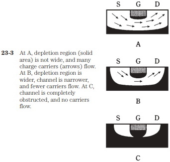
Either the N-channel or the P-channel JFET works because the voltage at the gate causes an electric field that interferes, more or less, with the flow of charge carriers along the channel. A simplified drawing of the situation for an N-channel device is shown in Fig. 23-3. For a P-channel device, just interchange polarity (minus/plus) and semiconductor types (N/P) in this discussion.
As the drain voltage ED increases, so does the drain current ID, up to a certain level-off value. This is true as long as the gate voltage EG is constant, and is not too large negatively.
But as EG becomes increasingly negative (Fig. 23-3A), a depletion region (solid black) begins to form in the channel. Charge carriers cannot flow in this region; they must pass through a narrowed channel. The more negative EG becomes, the wider the depletion region gets, as shown at B. Ultimately, if the gate becomes negative enough, the depletion region will completely obstruct the flow of charge carriers. This is called pinchoff, and is illustrated at C.
Again, think of the garden-hose analogy. More negative gate voltages, EG, correspond to stepping harder and harder on the hose. When pinchoff takes place, you've cut off the water flow entirely, perhaps by bearing down with all your weight on one foot! Biasing beyond pinchoff is something like loading yourself up with heavy weights as you balance on the hose, thereby shutting off the water flow with extra force.

JFET biasing
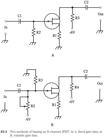
Two biasing arrangements for an N-channel JFET are shown in Fig. 23-4. These hookups are similar to the way an NPN bipolar transistor is connected, except that the source-gate (SG) junction is not forward-biased.
At A, the gate is grounded through resistor R2. The source resistor, R1, limits the current through the JFET. The drain current, ID, flows through R3, producing a voltage across this resistor. The ac output signal passes through C2.
At B, the gate is connected to a voltage that is negative with respect to ground through potentiometer R2. Adjusting this potentiometer results in a variable negative EG between R2 and R3. Resistor R1 limits the current through the JFET. The drain current, ID, flows through R4, producing a voltage across it; the ac output signal passes through C2.
In both of these circuits, the drain is positive relative to ground. For a P-channel JFET, reverse the polarities in Fig. 23-4. The connections are somewhat similar to the way a PNP bipolar transistor is used, except the SG junction isn't forward-biased.

Typical JFET power supply voltages are comparable to those with bipolar transistors. The voltage between the source and drain, abbreviated ED, can range from about 3 V to 150 V; most often it is 6 V to 12 V.
The biasing arrangement in Fig. 23-4A is commonly used for weak-signal amplifiers, low-level amplifiers and oscillators. The scheme at B is more often employed in power amplifiers having a substantial input signal.
About the Author
Stan Gibilisco is one of McGraw-Hill's most prolific and popular authors, specializing in electronics and science topics. His clear, reader-friendly writing style makes his science books accessible to a wide audience, and his background in research makes him an ideal editor for professional references and course materials. He is the author of The Encyclopedia of Electronics; The McGraw-Hill Encyclopedia of Personal Computing; and several titles in the popular Demystified library of home-schooling and self-teaching books. His published works have won numerous awards. The Encyclopedia of Electronics was chosen a "Best Reference Book of the 1980s" by the American Library Association, which also named his McGraw-Hill Encyclopedia of Personal Computing a "Best Reference of 1996." Stan Gibilisco maintains a Web site at www.sciencewriter.net.
Quickly and easily learn the hows and whys behind basic electricity, electronics, and communications - at your own pace, in your own home Teach Yourself Electricity and Electronics, Fourth Edition offers easy-to-follow lessons in electricity and electronics fundamentals and applications from a master teacher, with minimal math, plenty of illustrations and practical examples, and test-yourself questions that make learning go more quickly. Great for preparing for amateur and commercial licensing exams, this trusted guide offers uniquely thorough coverage, ranging from dc and ac concepts and circuits to semiconductors and integrated circuits.
The best course - and source - in basic electronics
• Starts with the basics and takes you through advanced applications such as radiolocation and robotics
• Packed with learning-enhancing features: clear illustrations, practical examples, and hundreds of test questions
• Helps you solve current-voltage-resistance-impedance problems and make power calculations
• Teaches simple circuit concepts and techniques for optimizing system efficiency
• Explains the theory behind advanced audio systems and amplifiers for live music
• Referenced by thousands of students and professionals
• Written by an author whose name is synonymous with clarity and practical sense
New to This Edition: Updated to reflect the latest technological advances in:
• Wireless technology
• Computers and the Internet
• Transducers
• Sensors
• Robotics
• Audio systems
• Navigation
• Radiolocation
• Integrated circuits
ReaderRobert L. Young says; "I'm doing course development for a community college. I have evaluated a number of books in order to select one to use as the textbook. The course title is "Basic Electronics and Troubleshooting." This is the book I selected for the course. It has all of the material needed for the course requirements. It has good, understandable illustrations. It includes end of chapter quizzes with answers in the back. The book has far more material than we will be covering in the class, and includes more advanced math than the students will need for this particular course, but I don't see that as a disadvantage. I'll give them reading assignments relevant to the course work, and let them know that the book contains a lot of valuable, additional information for more advanced study. When I say "more advanced study," don't get me wrong; this book isn't a text for a graduate engineering course. It does, however, contain substantially more information than can be covered in a 72 hour Basic Electronics class. All the basics are well-covered and understandable, and the book allows you to keep moving forward from there."


