

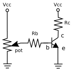
Shown above is a schematic with the symbol for an NPN transistor. The small arrow identifies the transistor's emitter. In this circuit, the transistor's collector is connected to the positive supply voltage through a resistor. It's emitter is connected to ground. Its base is connected through a resistor to the wiper of a potentiometer allowing an adjustable voltage to be applied. This configuration is referred to as a Common Emitter amplifier.
In an NPN transistor, the connection between base and collector is a PN junction, so it has similar properties as a PN junction in a diode. If the potentiometer is adjusted to the grounded end, the transistor would be turned off, and no current would flow. When the voltage from the potentiometer is set to 0.6 V between the base and emitter, it also starts to conduct. A small current flows into the base, and this results in a larger current flowing from emitter through the collector.
The ratio between base current and the collector current is the transistor's gain. For example, if a base current of 1 mA results in a collector current of 100 mA, the transistor would have a gain of 100.
When the base voltage is just over 0.6 V, a small current, not much as the transistor is barely turned on, flows from the emitter through to the collector. As the potentiometer voltage increases, the base voltage increases, and there will be a corresponding increase in the emitter through to the collector current.
There will be a range of base voltage through which the relationship between base current and collector current is almost linear. Eventually a base voltage will be reached where the collector current stops increasing no matter how much you increase the base current. At this base voltage the transistor is said to be saturated. The transistor is fully turned on, its current that's limited by the collector resistor.
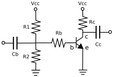
To design an amplifier circuit, we replace the potentiometer with a voltage divider with resistors selected to set the base voltage at the center of the transistor's linear region. Then, through a DC blocking capacitor, we apply a waveform to the transistor's base.
As the waveform voltage rises and falls, so does the base voltage, and thus the base current. And with the DC base voltage being held in the linear region, the voltage range of the applied waveform will be increased by the gain of the transistor. Because there is a resistor between collector and the supply, the amplified signal at the collector will be an inverted version of the signal provided at the base.

More Science, Technology, Engineering, and Mathematics Information:
• Properties of Algebra
• Lithium Ion Battery Chemistry
• How to Observe Constellations
• Average Velocity and Instantaneous Velocity
• Basic Geometry Terminology: Point, Line, Line Segment, Ray, Plane, Plane Figure
• What Is an Electronic Circuit?
• How to Add or Subtract Vectors
• Direct Current
• Electromagnetic Devices
• The Basic Concepts of Thermodynamics