
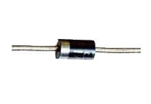
A diode is a semiconductor component designed to allow current to pass in one direction (the diode's forward direction), while blocking it in the opposite direction (the diode's reverse direction).
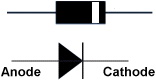
Above is the schematic symbol for a diode. When the voltage on the diode's anode is approximately 0.7 volts (for silicon, 0.3 volts for germanium) more positive than it's cathode, the diode will conduct current.
In the previous section we described how some elements, specifically germanium and silicon, although insulators in their pure form, can be made to conduct when "doped" with another element such as arsenic or gallium. For example, doping silicon with arsenic causes the crystal to have free electrons, this creates an "N type" semiconductor. Doping silicon with gallium causes the crystal to have a deficiency of electrons creating "holes", this creates "P type" semiconductor.
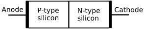
When a P type semiconductor joined with an N type of the same semiconductor element, what is called a diode is formed. When a P-N junction is formed, some of the free electrons in the N-region diffuse across the junction and occupy holes in the P-region.
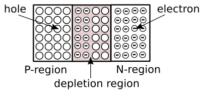
Electrons that moved to the P-type semiconductor create positive ions in the N-type side, while holes created in the N-type side create negative ions. This results in an electron field at the junction, forming a depletion region.
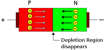
image adapted from wikibooks.org
In forward bias the P-region of the diode is connected to the positive voltage source and the N-region is connected to the negative. The positive voltage source draws electrons from the P-region, creating more holes. The negative voltage source pushes electrons into the N-region. The excess charge in the P and N regions will shrink the depletion region.
As the voltage increases the depletion region becomes thinner and at a specfic voltage called Vf (threshold voltage) the depletion layer disappears and the diode starts to conduct.
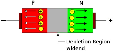
image adapted from wikibooks.org
In reverse bias the P-region is connected to the negative voltage source and the N-region is connected to positive. Holes in P-region get filled by electrons (in other words holes get removed from the diode). Electrons in the N-region are removed from the diode by the positive voltage source.
The depletion layer widens and occupies the entire diode. The resistance offered by the diode is high, and the diode will not conduct current.
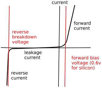
diode characteristics curve
The forward voltage drop across a diode varies only a little with the current. It is also varies as a function of temperature. If the reverse voltage across a diode reaches a value called the breakdown voltage, the diodes resistance to current flow suddenly drops and a high current called "avalanche current" will flow.
A special type of diode called a zener diode is designed to allow current to flow in reverse when a specific reverse voltage, known as the zener voltage, is reached. The zener voltage is controlled by amount of doping used in the P-N junction. Zener diodes are used for setting reference voltages and as surge suppressors. A zener circuit usually has a series resistor to limit the current, and drop the excess voltage when the diode is reverse conducting.

More Science, Technology, Engineering, and Mathematics Information:
• Electronics Lab
• Adding Vectors - Components of Vectors
• Electromagnetic Devices
• Projectile Motion
• Introduction to Angles: Acute, Obtuse, Straight, and Right
• Operational Amplifier
• Alternating Current
• Zener Diode
• Batteries
• EMI, RFI, EMC, EMS, What's the Difference?