
Over 1 million movies and TV episodes
Learn more at amazon.com

An integrated circuit (IC) is a thin rectangular piece of semiconductor upon which, using a photographic process, thousands of electronic components, and the conducting paths to connect them, are printed. The components that can be printed on a silicon chip are resistors, capacitors, diodes and transistors. By printing conducting paths on the chip, circuits like amplifiers, logic gates, and memory cells can be created.
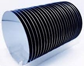
To make a silicon chip, first silicon is made extremely pure by heating it to over 1000 degrees centigrade in a crucible. The crucible is rotated slowly while the solidifying silicon is pulled in a cylindrical rod up to 12 inches in diameter. After the rod solidifies, a diamond saw is used to cut it into circular wafers 0.03 inches thick. The surfaces of the wafers are then polished flat to within 0.00008 inches, giving them a mirror-like finish.
To create electronic circuits on a wafer, it's heated in a furnace and exposed to pure oxygen which forms a silicon dioxide film of uniform thickness across the surface of the wafer. A layer of photoresistive film is applied to the surface of the wafer, giving it characteristics similar to photographic paper.
The wafer is then exposed to intense light through a mask. The mask defines the pattern of circuit features by protecting the areas where photoresist is to not be removed. The mask is much larger than the actual electronic circuits will be, so the pattern is projected through a reducing lens.
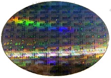
Silicon Wafer [Picture from Wikimedia Commons]
A developer solution is used to etch away the photoresist where the mask did not protect it from exposure to the light. A gaseous stream of dopant element atoms is directed at the exposed areas of the wafer causing the dopant atoms to embed themselves into the silicon. This creates the n-type and p-type regions.
The masking, exposing, etching, and doping steps are repeated several times to create the different circuit layers of the chip. The individual circuits are interconnected using a series of metal depositions and dielectric film insulation depositions.

Chip Package [Picture from Wikimedia Commons]
After the last last layer of metal connection pattern is deposited, a final insulating layer of dielectric is deposited to protect the circuit. Openings are etched into this insulating film to allow the connection of contact leads.
Each wafer has hundreds of chips, a diamond saw is used to cut the wafer into individual chips. The chips are then assembled into a package that provides contact leads for the chip.
The types circuits that can be etched into a semiconductor chip range from amplifiers to logic gates and even microprocessors with millions of transistors.
More Science, Technology, Engineering, and Mathematics Information:
• The Gravitational Force
• How to Find the Andromeda Galaxy
• Lead-Acid Battery Chemistry
• How to Prepare Microscope Slides
• Circuit Analysis with Thevenin's theorem
• Electric Fields and Static Electricity
• Average Velocity and Instantaneous Velocity
• The Basic Concepts of Thermodynamics
• Alternating Current
• The Normal Force