An Overview of the Printed Circuit Board (PCB) Fabrication Process
By Randall Scasny

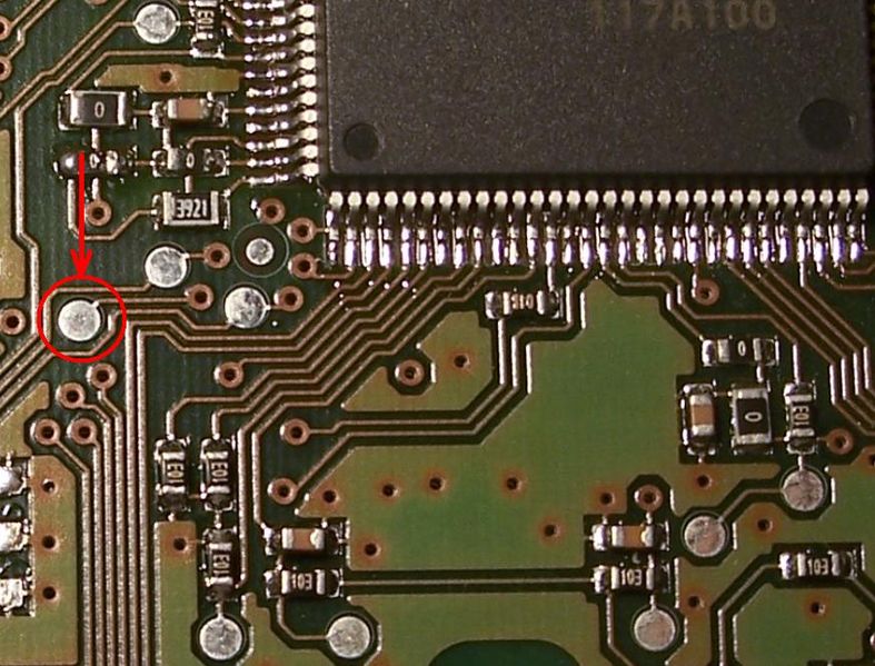
Printed Circuit Board (Creative Commons)
In 1936, the first printed circuit board (PCB) was created by Paul Eisle. But it wasn't
until the 1950s when the U.S. Defense industry began integrating PCBs in their bomb detonator
systems that printed circuit boards found wide application. PCBs are now used in nearly all
manufactured products such as, automobiles, cellular telephones, personal computers, among others.
A Summary of the PCB Fabrication Processes

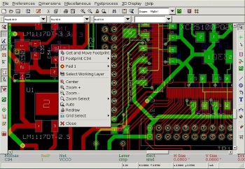
PCB Layout Application (Creative Commons)
PCBs are initially fabricated with the use of two types of software. Computer Aided Design
(CAD) software is used to design the electronic schematic of the circuit to be produced. After
the schematic is designed, Computer Aided Manufacturing (CAM) software is used by engineers
to produce the PCB prototype.
Once the PCB prototype is designed, the first step in the fabrication process is to select
the material of the printed circuit board. There are many different types of PCB materials
available, but the popular ones, based on the application and a customer's requirements, include:
Alumina, Arlon, Bakelite, CEM1, CEM5, Ceramic, FR1, FR4, FR4 High Temperature, GeTek, Nelco,
Polyimide and Rogers.The design requirement dictates the dimensions of the PCB (I.e., length,
width and thickness).
After the material has been selected, the first process is to apply a coating of copper
to the entire board. The circuit layout will then be printed on the board by a photosensitive
process. Then, a photo engraving process will be used so that all the copper that is not part
of the circuit layout will be etched out or removed from the board. The resulting copper creates
the traces or tracks of the PCB circuit. To connect the circuit traces, two processes are used.
A mechanical milling process will use CNC machines to remove the unnecessary copper from the
board. Then, an etch-resistant, silk-screen, printing process is applied to cover the regions
where traces must exist.
At this point in the PCB fabrication process, the PCB board contains copper traces without
any circuit components. To mount the components, holes must be drilled at the points where
the electrical and electronics parts are placed on the board. The holes are drilled with either
lasers or a special kind of drill bit made of Tungsten Carbide. Once the holes are drilled,
hollow rivets are inserted into them or they are coated by an electroplating process, which
creates the electrical connection between the layers of the board.
A masking material is then
applied to coat the entire PCB with the exception of the pads and the holes. There are many
types of masking material such as, lead solder, lead free solder, OSP (Entek), deep/hard gold
(electrolytic nickel gold), immersion gold (electroless nickel gold - ENIG), wire bondable
gold (99.99% pure gold), immersion silver, flash gold, immersion tin (white tin), carbon ink,
and SN 100CL, an alloy of tin, copper, and nickel. The final step in the PCB fabrication process
is to screen print the board so labels and the legend appear at their proper locations.
|

