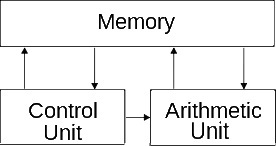
The basic architecture of almost every computer system ever made is based on the stored program architecture designed in 1945 design by the mathematician John Von Neumann.
He described a computer architecture where data and instructions would be stored in memory. A control unit with a program counter and an instruction register would fetch pieces of data from memory and, using an instruction set, determine if that data was an instruction, or data. If it was an instruction, it would execute that instruction.
An instruction might be to add two pieces of data together. In that case, the control unit would fetch the two pieces of data and move them into registers in the arithmetic logic unit (ALU) and send a control signal to the ALU causing it to add the data in the registers and store the result in a register.
A following instruction might be to store the result from the ALU register to a specific location in random access memory (RAM), a type of memory which can be read-from and written-to. Other instructions fetched from memory might be to get data from an input device, or send data to an output device.

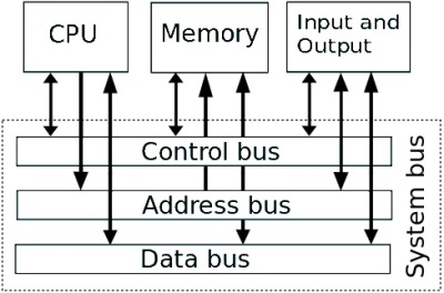
Above is shown how the stored program architecture has evolved into a system with a single system bus. Although this makes systems more practical from a physical construction point of view, it doesn't allow the system to fetch program instructions and access data at the same time. This limitation is sometimes referred to as the Von Neumann bottleneck.

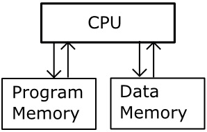
One method to alleviate the Von Neumann bottleneck is to divide the memory into two parts, one for program instructions, and one for data. Then the CPU can be fetching instructions and accessing data at the same time.
This method, requiring two buses, a program bus and a data bus, is often called the Harvard Architecture. However, there are always trade-offs and the Harvard Architecture would be more complex to program and more costly to manufacture.
Another method to alleviate the bottleneck is to place a cache between the CPU and the main memory. A cache is a small amount of RAM. When the CPU goes to access main memory, instead of just one piece of data, it moves a block of data into the cache. This allows the CPU to access the data in the cache and in the main memory at the same time. Today's CPU's use multiple levels of caches.
More Computer Architecture Articles:
• Digital Logic Levels and Transfer Characteristics
• Factors in Choosing an Oscilloscope
• Simplified Windows Architecture Overview
• The Many Processes of Silicon Wafer Manufacturing
• Dynamic Loading of Program Routines and Dynamically linked libraries (DLLs)
• Electronic Circuits
• Multicore Programming
• Pi-Top kit - Build Your Own Laptop
• Operating System File Management
• Intel's Sandy Bridge Micro-Architecture

