

General Description of the SPI
In synchronous serial communication, both the transmitter and receiver use the same synchronization clock to transfer data. Therefore, the device that generates the transmission clock fully controls the moment and the speed of the transmission, and it is called the MASTER.
The HC11 and AVR families of microcontrollers include a synchronous serial interface, called the Serial Peripheral Interface (SPI), allowing operation either in MASTER mode or in SLAVE mode. The general block diagram of a SPI link is presented in Fig. 4.1.
Four shift registers are involved in this link. All work with the same shift clock, generated by the MASTER device. The transmission and reception processes occur simultaneously. Two data line are provided to this purpose: MOSI – (MASTER Out SLAVE In) and MISO (MASTER In SLAVE Out).
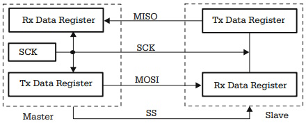
Fig. 4.1. General block diagram of a SPI link
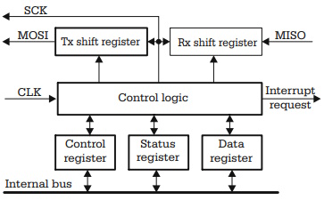
Fig. 4.2. General block diagram of the SPI
When the MASTER writes by software a byte into the transmitter's data register, eight clocks are automatically generated to the SCK line, and the bi-directional transmission begins. Whatever is found at this moment in the SLAVE's Tx Data Register is shifted into the MASTER's Rx Data Register.
When more than one SLAVE device is connected to the SPI bus, only one SLAVE may be enabled at a certain time. An additional signal SS (SLAVE Select), active LOW, is used to select the active SLAVE device.
The SPI of HC11 Microcontrollers
The structure of the SPI of HC11 follows exactly the general structure of a peripheral interface, shown in Fig. 1.6. The registers of the interface are called SPDR (SPI Data Register), SPCR (SPI Control Register), and SPSR (SPI Status Register).
SPDR - SPI Data Register
When writing to the address of SPDR, data is directly written into the transmitter’s shift register. Reading from this address actually reads the last byte received in the receivers shift register. SPDR is double buffered for input, and single buffered for output. This means that SPDR can be read while a data transfer is in progress, but if a byte is written into SPDR before the transmission of the previous character is completed, an error condition occurs.
SPSR - SPI Status Register
The status register has the following structure:
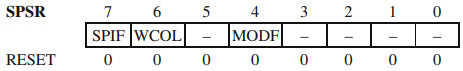
• SPIF : SPI transfer complete flag. This flag is set when a SPI transfer
is complete (after eight SCK cycles in a data transfer). It is cleared by reading SPSR
(with SPIF = 1), then accessing (reading or writing) SPDR.
SPIF = 0 No SPI transfer complete or SPI transfer still in progress
SPIF = 1 SPI transfer complete
• WCOL : Write Collision. This is an error flag. It is set if the software tries to
write data into SPDR while SPI data transfer is in progress. Clear this flag by
reading SPSR (WCOL = 1), then access SPDR.
WCOL = 0 No write collision
WCOL = 1 Write collision
• MODF : Mode Fault. This is another error flag. This error occurs when the input
line SS is pulled LOW (the device is hardware configured as SLAVE) while the
bit MSTR in the control register SPCR is set to 1.
MODF = 0 No mode fault
MODF = 1 Mode fault
This type of error occurs in multi-MASTER networks when more than one device is trying to become MASTER at a certain moment.
All other bits of SPSR are not implemented and always read 0. Out of RESET, SPSR is cleared.
Using the SPI To Connect Two Microcontrollers
The SPI is a fast data communication link. It is not designed to work over long distances. SPI can be used to create networks with two or more microcontrollers, when processing tasks are distributed between two or more microcontrollers for faster processing, or to connect special memory or peripheral devices.
A typical hardware SPI connection between two HC11E9 microcontrollers is shown in Fig. 4.3. In all situations, it is important to define a communication protocol between the two devices.
If, for instance, the SLAVE device is used to expand the MASTER's I/O space with two input ports, then the MASTER should send al least three bytes through the SCI: the first byte is an opcode needed to inform the SLAVE about the intention of the MASTER to read data from the SLAVE's ports, and two other dummy bytes must be sent in order to generate the clock pulses needed to read the two data bytes from SLAVE.
Note that the SLAVE device does not have any initiative in a SPI link - it's the MASTER that decides when to start the communication, and how many data bytes are to be exchanged between the two devices.
A convenient way to write the software is to write an interrupt-driven SPI communication routine for the SLAVE, like in the example below:
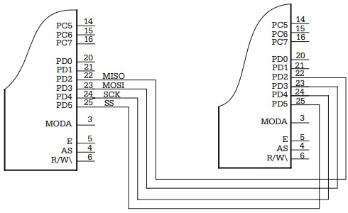
Fig. 4.3. SPI link between two 68HC11E9 microcontrollers
Expanding the I/O Space Using the SPI
In some cases, when the number of MCU I/O lines is insufficient for a certain application, a possible solution to expand the I/O space is to use shift registers connected to the SPI. The following example shows how the I/O space of an ATMega8 AVR is expanded with one 8-bit input port, and one 8-bit output port. For the input port, a parallel-input serial-output shift register (74165) is used. The output port is implemented using a 4094 serial-input parallel-output register. The schematic of the circuit is presented in Fig. 4.4.
Obviously, in this SPI link, the MASTER device is the microcontroller. The serial data input of register IC2 is connected to the MOSI line of the MCU. The shift clock for this register is generated by the microcontroller on the SCK line. The load (LD) input for the 4094 register is driven by an extra output line of the micrcontroller (PB2).
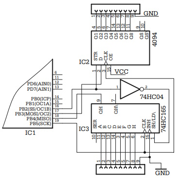
Fig. 4.4. Expanding the I/O space of ATMega8 using the SPI
When the microcontroller writes a byte into SPDR, eight clock pulses are automatically generated on the SCK line, and the content of SPDR is presented to the MOSI line, bit by bit, and shifted into IC2. When the serial transfer completes, the data in IC2 is effectively transferred to the output lines by generating a pulse 0-1-0 on LD (PB2).
The load signal SH/LD\ of the 4094 circuit is active LOW. This signal is obtained by inverting the LD signal with the gate IC6. When 74C165 senses an active LOW pulse on the SH/LD\ input, the status of the input lines is latched into the shift register, and will be shifted into the microcontroller through the MISO line on the same clock pulses SCK used to refresh the status of output registers. The processes of transmission of output data and reception of input data are simultaneous.
The software must do the following steps:
1. Generate a pulse on LD (SH/LD\) to strobe the input lines into 74C165.
2. Write the output data into SPDR.
3. Poll SPIF waiting for the end of transfer.
4. Read the input byte from SPDR, and save it into a variable.
5. Generate another pulse on LD to strobe the output data onto the parallel lines.
About Microcontrollers in Practice

The book is structured into three sections. Chapters 1-8 aim to create a detailed overview of microcontrollers, by presenting their subsystems starting from a general functional block diagram, valid for most microcontrollers on the market. In each case, we describe the distinctive features of that specific subsystem for HC11, 8051 and AVR. This whole section has a more theoretical approach, but, even here, many practical examples are presented, mainly regarding the initializations required by each subsystem, or the particular use of the associated interrupts. The purpose of this section is to create a perspective that views the microcontroller as a set of resources, easy to identify and use.
Chapters 9-16 contain eight complete projects, described from the initial idea, to the printed circuit board and detailed software implementation. Here too, we permanently focus on the similarities between the microcontrollers discussed, from the hardware and software perspectives.
All chapters contain exercises, suggesting modifications or improvements of the examples in the book. Most exercises have solutions in the book; for the others the solutions can be found on the accompanying CD.
Finally, the appendices contain additional information intended to help the reader to fully understand all the aspects of the projects described in the previous sections. We chose to present these details separately in these appendices, in order to avoid fragmentation of the flow of the main text.
Stressing common characteristics and real applications of the most used microcontrollers, this practical guide provides readers with hands-on knowledge of how to implement three families of microcontrollers (HC11, AVR, and 8051). Unlike the rest of the ocean of literature on individual chips, Microcontrollers in Practice supplies side-by-side comparisons and an overview that treats the systems as resources available for implementation. Packed with hundreds of practical examples and exercises to foster mastery of concepts and details, the guide also includes several extended projects. By treating the less expensive 8-bit and RISC microcontrollers, this information-dense manual equips students and home-experimenters with the know-how to put these devices into operation. Click here to learn more.

More Computer Architecture Articles:
• Digital Logic Semiconductor Families
• CPU Process Memory Address Binding
• Intel's Core 2 Processors
• Microcontroller Architectures
• The Fetch, Decode, Execute Cycle
• Operating System Process Control Block
• AMD Sempron Processor
• Operating System Memory Paging Hardware Support
• Intoduction to Digital Electronics
• Operating System Services