

The digital I/O lines are the simplest and most common way microcontrollers interact with the outside world. Figure 2.1 shows how digital input and output lines are connected to the internal bus of the MCU.
In case of an input line, the status of the MCU pin is transferred on the internal bus to the CPU by activating the internal signal RP (Read Port), generated during the execution of the instruction used to read the port.
An output line is associated with an internal latch, which can be written from the internal bus and the driver connected to the physical pin.
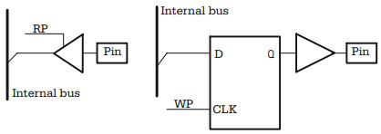
Fig. 2.1. The principle of accessing the input and output lines
In practice, things are a bit more complicated. For economic and technological reasons, it is more convenient to assign two or more functions to each pin than to double the number of pins of the capsule. This is the reason why all microcontrollers extensively use bi-directional input/output lines. The simplest way to obtain a bidirectional line is to use an open drain driver for the output line. When the output transistor is blocked, an external device can control the line. Figure 2.2 shows the logic diagram of a bi-directional I/O line implemented according to this principle.
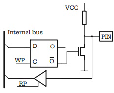
Fig. 2.2. Bi-directional I/O line with open drain output driver
When the software writes 1 to the latch associated with the output line, the output transistor is blocked, and the line is turned into an input line. This solution is used by the 8051 microcontrollers.
Another way to do this is to associate to each bi-directional I/O line an additional latch, called a direction latch, which controls a tri-state output driver. When the direction latch is set to 1 by software, the I/O line is configured as an output line. A simplified logic diagram of an I/O line implemented according to this principle is shown in Fig. 2.3.
This method of controlling the direction of the I/O lines is characteristic of the microcontrollers belonging to the HC11 and AVR families.
Usually, the I/O lines are grouped into 8-bit ports, which have individual addresses in the memory map. Similarly, the direction control bits are grouped into 8-bit registers, called Data Direction Registers (DDR), associated with each I/O port.
Note that the I/O port, along with the associated data direction register, form a structure similar to the general structure of the I/O peripheral interface, shown in Fig. 1.6, where the data register is the port itself, and the control register is the data direction register.
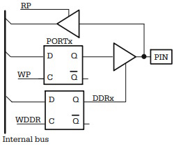
Fig. 2.3. Bi-directional I/O line with direction control
Often, the I/O lines have alternate functions in connection with some of the microcontroller’s subsystems. For example, the asynchronous serial interface of the HC11 uses the lines of port D, and the timer subsystem can use the lines of port A. Normally, the external pins are automatically configured for the alternate function when the respective subsystem is enabled by software, overriding the settings in the data direction register, but this is not an absolute rule. Refer to the data sheet of each microcontroller for details on how a certain peripheral interface shares the MCU pins with the I/O ports.
Electrical Characteristics of the I/O Lines
One simple rule about interfacing a microcontroller is that any output line can safely drive one standard TTL load, and the voltage on any input may swing between the potential of GND and Vdd. In some particular cases, certain output lines can drive up to 20 mA each, but even in these cases, care must be taken that the total power dissipation does not exceed the limit specified by the manufacturer.
If the load current or voltage requirements are higher than the capabilities of the microcontroller, the solution is to use adequate buffers between the control circuit and the load. Figure 2.4 shows a possible way to connect a relay to an output line of the 68HC11F1 microcontroller.
The relay is driven by the CMOS circuit 40107, able to drain a current up to 100 mA. Note the presence of the pull-down resistor R1, which connects the MCU output to the ground. Its purpose is to maintain the line at the stable potential of ground during RESET.
This is required because, at RESET, all the I/O lines of the microcontroller are automatically configured as input lines. In the time interval between RESET and the moment when the I/O line is configured as output, the potential at the input of the 40107 is undetermined, and thus the relay can be unintentionally activated.
The value of the pull-down resistor is determined by the fact that it loads the MCU output line, which can supply a maximum current of 8–1 mA. A value of 10 K for this resistor loads the output line with 0.5 mA and provides a safe pull-down for the input of 40107.
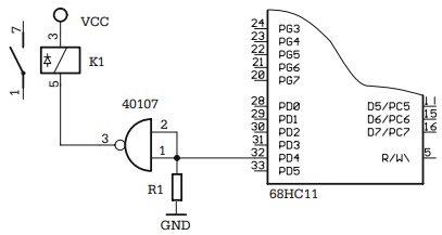
Fig. 2.4. Connecting a relay to an output line of a microcontroller
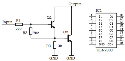
Fig. 2.5. ULN 2803 typical Darlington transistor interface for output lines
When higher current values are required, Darlington transistors are recommended to connect the load. Figure 2.5 shows the schematic of a Darlington driver, as implemented in the circuit ULN2803. This contains an array of eight such Darlington drivers, each being able to sink 500 mA current and to stand 50 V VCE voltage.
As far as the input lines are concerned, the most common way of using them is to read the status of contacts (push buttons, relays, etc.). The interface circuits must provide precise logic levels for each possible status of the contact, and to eliminate, as much as possible, the mechanical vibrations of the contact. A typical interface circuit for digital input lines is presented in Fig. 2.6.
R1 is a pull-up resistor, intended to maintain a stable logic level high, when the contact is open. Typical values are in the range 4.7 K–10 K. The capacitor C1, and the Schmitt trigger 40106 are destined to eliminate the effect of the vibrations of the contact, and to create clean edges for the electrical signal applied to the MCU port.
Often, it is required that the MCU ground be separated from the ground of the input circuits. In this case, it is recommended that the input lines are optically isolated, using circuits similar to that presented in Fig. 2.7. In this circuit, the resistor R1 limits the current through the LED of the optocoupler OK1. When K1 is closed, the transistor of the optocoupler saturates, providing a logic level zero at the input line of the microcontroller. The role of R3 is to drain the charge accumulated in the parasite capacitance of the junction BE of the transistor, thus improving the rising edge of the signal in the collector. Typical values for R3 are in the range 330 K–470 K.
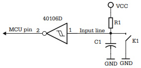
Fig. 2.6. Typical input circuit for reading relay contacts, push buttons, etc.
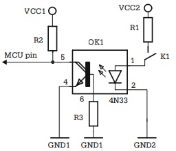
Fig. 2.7. Optically isolated input line
Controlling the I/O Lines by Software
The HC11 microcontrollers treat the I/O ports and the associated direction registers as memory locations. The software initialization of I/O lines consists in writing to the data direction register a byte having 1 in the positions corresponding to the output lines, like in this example:
INIT_PORTD LDAA #$30 ;configure PORTD, bit 4,5 as
STAA DDRD ;output
For HC11, the software can read a port configured as output. In this situation, the last value written to the port is read. Data written to an input port is not visible to the MCU pins until the port is reconfigured as an output port.
The 8051 microcontrollers have two major features, as far as the I/O ports are concerned: there are no direction registers, and the ports are bit-addressable.
All output pins of 8051 have open drain drivers, as shown in Fig. 2.2, and writing a 1 to the port configures the corresponding line as input. Special instructions for bit manipulation allow code sequences like this:
MOV C,P1.2 ;Move P1 bit2 to carry
MOV P1.3,C ;move carry bit to P1 bit 3
CLR P2.1 ;clear P2 bit 1
SETB P1.0 ;set bit 0 in P1
JB P3.3,LABEL ;Jump to LABEL if P3 bit 3 is set
The I/O subsystem of the AVR microcontrollers have some interesting distinctive features (refer to Fig. 2.8). First, note the presence of two data registers, having distinct addresses, associated with each port: one, called PINx, is used when the port is configured as input, and the other, called PORTx, is used when the port is configured as output.
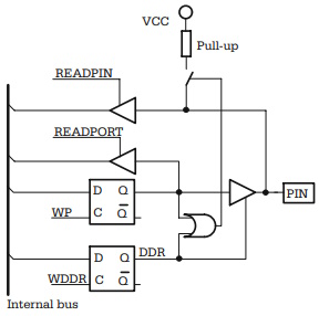
Fig. 2.8. Distinctive Features of the I/O lines of the AVR
Writing to PORTx when DDRx = 0 (i.e. when the port is configured as input) connects internal pull-up resistors to the input lines corresponding to the bits in PORTx set to 1.
The actual status of the input lines is obtained by reading from the address PINx. Reading from the address PORTx, when the port is configured as output, returns the last value written to the port.
Special instructions have been provided to allow software access to the I/O ports or to the individual bits thereof. These are:
IN Rd,ioport ;read from the address ioport to ;register Rd
OUT ioport,Rs ;write data from Rs to ioport
SBI ioport,bit ;set specified bit to ioport
CBI ioport,bit ;clear specified bit to ioport
The following program fragment illustrates aspects of the configuration and access to PORTB:
LDI R16, $F0 ;configure upper nibble of PORTB ;as output
OUT DDRB,R16
LDI R16,$0F
OUT PORTB,R16 ;enable internal pull-ups on ;lower nibble and write 0 in the
;upper nibble
IN R0,PINB ;read the input lines
About Microcontrollers in Practice

The book is structured into three sections. Chapters 1-8 aim to create a detailed overview of microcontrollers, by presenting their subsystems starting from a general functional block diagram, valid for most microcontrollers on the market. In each case, we describe the distinctive features of that specific subsystem for HC11, 8051 and AVR. This whole section has a more theoretical approach, but, even here, many practical examples are presented, mainly regarding the initializations required by each subsystem, or the particular use of the associated interrupts. The purpose of this section is to create a perspective that views the microcontroller as a set of resources, easy to identify and use.
Chapters 9-16 contain eight complete projects, described from the initial idea, to the printed circuit board and detailed software implementation. Here too, we permanently focus on the similarities between the microcontrollers discussed, from the hardware and software perspectives.
All chapters contain exercises, suggesting modifications or improvements of the examples in the book. Most exercises have solutions in the book; for the others the solutions can be found on the accompanying CD.
Finally, the appendices contain additional information intended to help the reader to fully understand all the aspects of the projects described in the previous sections. We chose to present these details separately in these appendices, in order to avoid fragmentation of the flow of the main text.
Stressing common characteristics and real applications of the most used microcontrollers, this practical guide provides readers with hands-on knowledge of how to implement three families of microcontrollers (HC11, AVR, and 8051). Unlike the rest of the ocean of literature on individual chips, Microcontrollers in Practice supplies side-by-side comparisons and an overview that treats the systems as resources available for implementation. Packed with hundreds of practical examples and exercises to foster mastery of concepts and details, the guide also includes several extended projects. By treating the less expensive 8-bit and RISC microcontrollers, this information-dense manual equips students and home-experimenters with the know-how to put these devices into operation. Click here to learn more.

More Computer Architecture Articles:
• Operating System Memory Protection in a Paged Environment
• Intel Celeron D Processor
• Intel's Core 2 Processors
• Introduction to the Raspberry Pi
• Operating System Process Control Block
• Load Balancing Multiple CPUs in Symmetric Multiprocessing
• Shortest-Job-First CPU Scheduling Algorithm
• Operating System Memory Management
• Binary Number Representation and Binary Math
• Intel's Sandy Bridge Micro-Architecture