The following is an excerpt from Digital Design and Computer Architecture: ARM Edition
Logic Levels
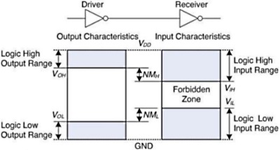
The mapping of a continuous variable onto a discrete binary variable is done by defining logic levels, as shown in figure 1.23. The first gate is called the driver and the second gate is called the receiver. The output of the driver is connected to the input of the receiver. The driver produces a LOW (0) output in the range of 0 to VOL or a HIGH (1) output in the range of VOH to VCDD. If the receiver gets an input in the range of of 0 to VIL, it will consider the input to be LOW. If the receiver gets an input in the range of VIH to VCDD, it will consider the input to be HIGH. If for some reason such as noise or faulty components, the receiver's input should fall in the forbidden zone between V,IL and VIH, the behavior of the gate is unpredictable. VOH, VIH, VOL, and VIL are called the output and input high and low logic levels.

figure 1.23
Noise Margins
If the output of the driver is to be correctly interpreted at the input of the receiver, we must choose VOL < VIL and VOH > VIH. Thus, even if the output of the driver is contaminated by some noise, the input of the receiver will still detect the correct logic level. The noise margin is the amount of noise that could be added to a worse-case output such that the signal can still be interpreted as a valid input. As can be seen in Figure 1.23, the low and high noise margins are respectively
NML = VIL - VOL
NMH = VOH - VIH
VDD stands for the voltage on the drain of a metal-oxide-semiconductor transistor, used to build most modern chips. The power supply voltage is also sometimes called VCC, standing for the voltage on the collector of a bipolar junction transistor used to build chips in older technology. Ground is sometimes called VSS because it is the voltage on the source of a metal-oxide-semiconductor transistor.
DC indicates behavior when an input voltage is held constant or changes slowly enough for the rest of the system to keep up. The term's historical root comes from direct current, a method of transmitting power across a line with a constant voltage. In contrast, the transient response of a circuit is the behavior when an input voltage changes rapidly.
DC Transfer Characteristics
To understand the limits of the digital abstraction, we must delve into the analog behavior of a gate. The DC transfer characteristics of a gate describe the output voltage as a function of the input voltage when the input is changed slowly enough that the output can keep up. They are called transfer characteristics because they describe the relationship between input and output voltages.
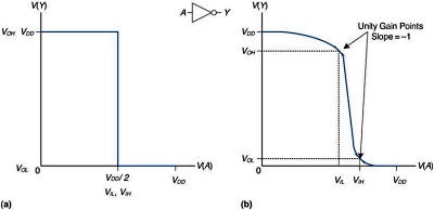
An ideal inverter would have an abrupt switching threshold at VDD/2, as shown in figure 1,25.(a). For V(A) < VDD/2, V(Y) > VDD/2, V(Y) = 0. In such a case, VIH = VIL = VDD/2. VOH = VDD and VOL = 0.

figure 1.25
A real inverter changes more gradually between the extremes, as shown in Figure 1.25b. When the input voltage V(A) is 0, the output voltage V(Y) = VDD. When V(A) = VDD, V(Y) = 0. However, the transition between these endpoints is smooth and may be centered at exactly VDD/2. This raises the question of how to define the logic levels. A reasonable place to choose the logic levels is where the slope of the transfer characteristic dV(y)/dV(A) is -1. These two points are called the Unity gain points. Choosing logic levels at the unity gain points usually maximizes the noise margins. If VIL were reduced, VOH would only increase by a small amount. But if VIL were increased, VOH would drop precipitously.
The Static Discipline
To avoid inputs falling into the forbidden zone, digital logic gates are designed to conform to the static discipline. The static discipline requires that, given logically valid inputs, every circuit element will produce logically valid outputs.
By conforming to the static discipline, digital designers sacrifice the freedom of using arbitrary analog circuit elements in return for the simplicity and robustness of digital circuits. They raise the level of abstraction from analog to digital, increasing design productivity by hiding needless detail.
The choice of VDD and logic levels is arbitrary, but all gates that communicate must have compatible logic levels. Therefore, gates are grouped into logic families such that all gates in a logic family obey the static discipline when used with other gates in the family. Logic gates in the same logic family snap together like Legos in that they use consistent power supply voltages and logic levels.
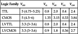
Four major logic families that predominated from the 1970's through the 1990's are Transistor-Transistor Logic (TTL), Complementary Metal-Oxide-Semiconductor Logic (CMOS, pronounced sea-moss), Low Voltage TTL Logic (LVTTL), and Low Voltage CMOS (LVCMOS). Their logic levels are compared in Table 1.4. Since then, logic families have balkanized with a proliferation of even lower power supply voltages.

Table 1.4
Digital Design and Computer Architecture: ARM Edition takes a unique and modern approach to digital design. Beginning with digital logic gates and progressing to the design of combinational and sequential circuits, Harris and Harris use these fundamental building blocks as the basis for what follows: the design of an actual ARM processor. With over 75% of the world's population using products with ARM processors, the design of the ARM processor offers an exciting and timely application of digital design while also teaching the fundamentals of computer architecture. SystemVerilog and VHDL are integrated throughout the text in examples illustrating the methods and techniques for CAD-based circuit design. By the end of this book, readers will be able to build their own microprocessor and will have a top-to-bottom understanding of how it works. Harris and Harris have combined an engaging and humorous writing style with an updated and hands-on approach to digital design.
More Computer Architecture Articles:
• Introduction to Microprocessor Programming
• Factors in Choosing an Oscilloscope
• Real-Time CPU Scheduling
• Computer Video Display
• Operating System Memory Allocation Methods
• Basic Decoder Circuitry
• Digital Logic Semiconductor Families
• Load Balancing Multiple CPUs in Symmetric Multiprocessing
• Microcontroller Architectures
• Stored Program Architecture

