In this article I explain the fundamental concept of digital logic in simple and clear language so that anyone can understand it Lets look at a simple electric circuit with a battery, a light bulb, and a switch. This circuit is shown below.
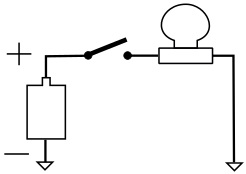
With the switch open, the light bulb does not illuminate.
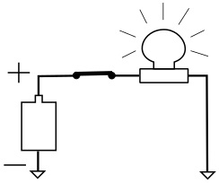
With the switch closed, the light bulb illuminates.
Lets designate the situation where the light is off as "0". Lets designate the situation were the light is illuminated as "1". What we have is a system with two possible situations, referred to as a "binary" system.
It doesn't matter what voltage the battery is, as long as its high enough to illuminate the light. Light off is binary 0. Light on is binary 1.
Lets make a slightly more complex circuit.
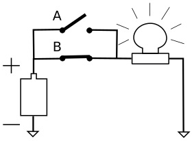
In the circuit shown above, switch A is open, but the light is still illuminated. That's because switch B is closed, providing a path from the battery to the light.
The idea behind this circuit is - if switch A OR switch B is closed, the light is illuminated. If both switched are open, the light will not be illuminated. Of course if both switched are closed the light will be illuminated.
This circuit functions as what we call a logical OR gate.
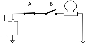
In the circuit shown above, switch A is closed, but the light is not illuminated. This is because switch B is open, breaking the path to the battery. If switch B were to be closed, the light would be illuminated because then there would be a closed path from the battery to the light.
If either switch is open, the light will not be illuminated. Both switch A AND switch B must be closed for the light to be illuminated.
This circuit functions as a logical AND gate.
These circuits demonstrate the fundamental concept of logic circuits.
Let's substitute the symbol shown below for the logical OR gate function.

If voltage is applied (a logical 1) to either A OR B (or both), voltage (a logical 1) will appear at the output. If neither input is 1, the output will be 0. The following table describes the logical OR function.
| A | B | Out |
| 0 | 0 | 0 |
| 0 | 1 | 1 |
| 1 | 0 | 1 |
| 1 | 1 | 1 |
This table is called a "truth table". It is the truth table for a 2-input OR gate.
Let's substitute the symbol shown below for the logical AND gate function.

If a logical 1 is applied only to input A, or only to input B, the output will be 0. Both inputs must be 1 for the output to be 1. The following table describes the logical AND function.
| A | B | Out |
| 0 | 0 | 0 |
| 0 | 1 | 0 |
| 1 | 0 | 0 |
| 1 | 1 | 1 |
This is the truth table for a 2-input AND gate.
Let's introduce a very simple gate shown below.
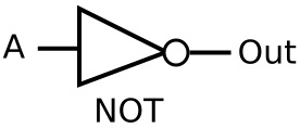
The output of this gate is always the binary opposite of the input. For example if A is 0, the output is 1. If A is 1, the output is 0. This describes the logical NOT function. many people just call it an "inverter". The following table describes the logical NOT function.
| A | Out |
| 0 | 1 |
| 1 | 0 |
Let's introduce one more gate before we move on to bigger things.

| A | B | Out |
| 0 | 0 | 0 |
| 0 | 1 | 1 |
| 1 | 0 | 1 |
| 1 | 1 | 0 |
A gate is not restricted to only 2 inputs. Shown below is a 3 input AND gate.

This is the truth table for a 3-input AND gate:
| A | B | C | Out |
| 0 | 0 | 0 | 0 |
| 0 | 0 | 1 | 0 |
| 0 | 1 | 0 | 0 |
| 0 | 1 | 1 | 0 |
| 1 | 0 | 0 | 0 |
| 1 | 0 | 1 | 0 |
| 1 | 1 | 0 | 0 |
| 1 | 1 | 1 | 1 |
Shown below is a 3 input XOR gate.

This is the truth table for a 3-input XOR gate:
| A | B | C | Out |
| 0 | 0 | 0 | 0 |
| 0 | 0 | 1 | 1 |
| 0 | 1 | 0 | 1 |
| 0 | 1 | 1 | 0 |
| 1 | 0 | 0 | 1 |
| 1 | 0 | 1 | 0 |
| 1 | 1 | 0 | 0 |
| 1 | 1 | 1 | 0 |
Be careful with the last line in this truth table. Many people have been cascading XOR gates to create the odd-parity checking function. They think the output of the last line should 1. XOR is logic gate, not an odd-parity checking gate. Apparently they don't understand the meaning of the word "exclusive". IEEE-Std91a-1991 gives the symbol for the exclusive-OR on p. 62 with the definition "The output stands at its 1 state if one and only one of the two inputs stands at its 1 state."
Shown below is a 2-input AND gate whose output is used as the input to a NOT gate. This creates the NAND function.

We don't actually need to construct such a circuit because this function is performed by a a NAND gate, the symbol of which is shown below.

This is the truth table for a 2-input NAND gate:
| A | B | Out |
| 0 | 0 | 1 |
| 0 | 1 | 1 |
| 1 | 0 | 1 |
| 1 | 1 | 0 |
As you can see the output of the NAND gate is the opposite of the AND gate. Why would they bother to put such a function as a fundamental gate? Actually combinations of NAND gates can be used to create any of the other basic logic functions. This makes the NAND gate one of the most useful logic gates.
Shown below is a 2-input OR gate whose output is used as the input to a NOT gate. This creates the NOR function.

We don't actually need to construct such a circuit because this function is performed by a NOR gate, the symbol of which is shown below.

| A | B | Out |
| 0 | 0 | 1 |
| 0 | 1 | 0 |
| 1 | 0 | 0 |
| 1 | 1 | 0 |
As you can see the output of the NOR gate is the opposite of the OR gate.
Shown below is an example of what those designers who have been cascading XOR gates to create the odd-parity checking function are doing.

| A | B | C | Y | Out |
| 0 | 0 | 0 | 0 | 0 |
| 0 | 0 | 1 | 0 | 1 |
| 0 | 1 | 0 | 1 | 1 |
| 0 | 1 | 1 | 1 | 0 |
| 1 | 0 | 0 | 1 | 1 |
| 1 | 0 | 1 | 1 | 0 |
| 1 | 1 | 0 | 0 | 0 |
| 1 | 1 | 1 | 0 | 1 |
To construct this logic table, you would first enter the values of Y based on A XORed with B. Then you would enter the Output values based on C XORed with Y. Note how that last output disagrees with the same out from the XOR logic table.
That concludes my explanation of fundamental digital logic gates. If you understood most of what is in this section, you are well on your way to becoming a digital logic designer. But in order to do that, you will want to get a working knowledge of Boolean Algebra, a mathematical technique to design complex logic circuits developed by English mathematician George Boole (1815 - 1864).
More Computer Architecture Articles:
• Network on a Chip (NoC)
• Microprocessor Registers
• Microprocessor Counter, Clock, Timer Circuits
• Dynamic Loading of Program Routines and Dynamically linked libraries (DLLs)
• Pi-Top kit - Build Your Own Laptop
• Operating System Processes
• Multilevel Queue CPU Scheduling Algorithm
• The Evolution of Hard Disk Bit Recording
• The Microcontroller's Asynchronous Serial Interface
• AMD's Phenom II Processor

