

An I2C bus (Inter IC bus) consists of two signal conductors named SDA (Serial Data) and SCL (Serial Clock) that interconnect at least two devices. Each of the devices connected to the bus must be identified by a unique address. In principle, any of the devices connected to the bus can transmit and receive data. The device that initiates and completes a bus transfer, and generates the transfer clock, is named the MASTER.
As any of the devices connected on the bus can become MASTER at a certain time, the SDA and SCL lines must both be bi-directional. In practice open drain or open collector lines are used. The pull-up resistors have usual values between 2 K and 10 K, depending on the chosen communication speed (at high speed, the pull-up resistor has a smaller value). The idle status of the SDA and SCL lines is HIGH. A bus transfer sequence comprises the following steps:
1. The MASTER device generates a START condition on the bus.
2. The MASTER device generates eight SCL pulses controlling the SDA line in
such a way that it transmits a byte which contains the SLAVE's device address
and codes the type of the transfer (writing or reading). The receiver samples the
SDA line while the SCL line is HIGH, and therefore data must be stable while
the SCL is HIGH. SDA may change status only when SCL is LOW.
3. The MASTER device sends a ninth clock on the SCL line, while releasing the
SDA data line. The device that recognized its address in the first byte transmitted
by the MASTER pulls the line LOW for the period of this clock, thus generating
an ACK (acknowledge) condition.
4. The MASTER device continues to generate packages of nine SCL pulses, while
the SDA is controlled either by the MASTER or by the SLAVE, depending on the
type of the transfer in course. After each byte transmitted, the receiver generates
an ACK condition. If the MASTER is the receiver (for example during a SLAVE
byte read operation), then THE MASTER will generate ACK.
5. The process continues until MASTER generates a STOP condition and the bus
returns to the idle status.
The following paragraphs describe each of the above steps.
The Start Transfer Condition
The START transfer condition consists of a HIGH to LOW transition of the SDA line, while the SCL clock line is maintained HIGH. The waveform corresponding to this condition is presented in Fig. 5.1.
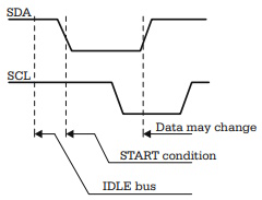
Fig. 5.1. The START TRANSFER condition on the I2C bus
The Data Transfer on the I2C BuS
The actual data transfer, after a START condition, begins after the SCL line is brought to LOW. At this moment, the state of the SDA data line may be modified and set to the value of the bit that follows in the transmission sequence. The receiver samples the SDA line only after the SCL line is raised HIGH. Figure 5.2 shows the waveforms for SDA and SCL for a transmission sequence containing the START condition, and the transmission of the four data bits in the sequence 1101. The first bit transmitted is the most significant bit (MSB) of each byte.
The ACK Bit
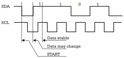
Fig. 5.2. Example of waveform for data transmission on the I2C bus
After the transmission of a byte (eight SCL pulses), the MASTER device releases the SDA line and generates a ninth SCL clock. When the SCL line becomes 1, the SLAVE device pulls SDA to LOW, confirming by this the reception of the byte. In all situations the data line is controlled by the receiver during the ACK bit time. In case of a read byte operation, the device that sends ACK is the receiver, i.e. the MASTER device.
The STOP Condition
A STOP transmission condition is generated when a LOW to HIGH transition of the SDA line occurs while the SCL line is HIGH. After the STOP condition, both SDA and SCL bus lines return to the idle state, and a new transmission must be preceded by a START sequence.
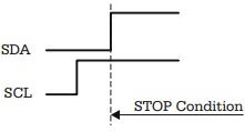
Fig. 5.3. The STOP TRANSFER condition on the I2C bus
In practice, the I2C protocol is more complicated, meaning that it allows operation in multimaster mode. In this case, an arbitration mechanism is required to allocate the bus in situations when two or more devices try to become MASTER at the same time. In this book only single-master I2C buses are discussed.
A Software Implementation of the I2C Protocol
There is a variety of circuits available, which are designed to communicate with a microcontroller via the I2C bus: memories, LCD displays, A/D and D/A converters, etc. Usually these are delivered in small capsules, with extremely low power consumption and require only two I/O lines of the microcontroller for connection.
Besides that, the access to any device connected to the I2C bus can be controlled by a library of reusable software modules. All these advantages recommend the I2C devices for many microcontroller applications, especially when the use of an expanded microcontroller structure is difficult or impossible.
The SDA and SCL lines are controlled by software through simple subroutines. The following example, written for HC11, illustrates the generation of the START condition on the I2C bus:
I2CSTART BSET PORTA,SCL ;make sure the clock is HIGH
JSR DELAY ;wait a few microseconds
BCLR PORTA,SDA ;HIGH to LOW transition of SDA
JSR DELAY
RTS
Similarly, a STOP condition is generated in the following way:
I2CSTOP BSET PORTA,SCL ;make sure the clock is HIGH
JSR DELAY ;wait a few microseconds
BSET PORTA,SDA ;LOW to HIGH transition of SDA
JSR DELAY
RTS
Accessing 24C256 Memory Devices
In the example presented in Fig. 5.4, the two 24Cxx circuits have the address lines A0, A1, A2, hardwired to different values. In this configuration, the microcontroller is, obviously, the MASTER device. After the START sequence, the microcontroller sends a byte that contains the address of the SLAVE device and the type of the operation: read or write. The structure of this byte is as follows:
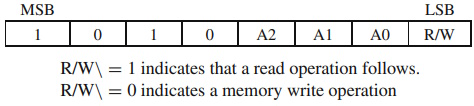
The upper-nibble of this byte is always 1010 for this type of memory. The A2, A1, A0 bits contain the SLAVE's device address. After the transmission of the byte with the SLAVE address, the device that recognizes its address pulls the SDA line LOW, for the duration of the ninth clock, thus generating the ACK condition.
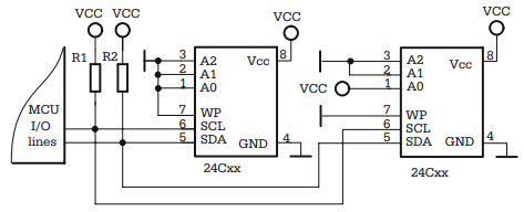
Fig. 5.4. Connecting I2C memory devices to a microcontroller
In the case of a write operation to the 24C256 memory, after the byte containing the SLAVE address, the microcontroller sends two bytes containing the address of the location that is to be written, followed by a byte containing the value to be written in the memory. After each received byte, the memory sends an ACK bit, and, after the last ACK, the microcontroller generates a STOP condition to complete the write operation. If, instead of generating a STOP condition, the microcontroller sends a new byte, this will be written in the memory to the next address. In this manner, up to 64 bytes can be written consecutively. This type of operation is named "page write mode".
To read a byte from a random address (random read operation) the microcontroller initiates a write sequence, in which it sends the byte with the SLAVE address, followed by two bytes with the address of the location that is to be read. Then, a new START is generated, followed by the SLAVE address byte, with the R/W\ bit set to 1, indicating a read operation. After the ACK is received from the SLAVE, the microcontroller sends eight more SCL pulses to get the read byte from memory, then it generates a STOP condition.
If, instead of generating the STOP condition, the microcontroller sends an ACK, followed by eight SCL clock pulses, it reads the byte from the next address. The process continues in the same way. At each ACK generated by the microcontroller, the internal address counter of the memory is incremented, and the process continues with reading of the next byte. The process completes when MCU generates a STOP condition.
About Microcontrollers in Practice

The book is structured into three sections. Chapters 1-8 aim to create a detailed overview of microcontrollers, by presenting their subsystems starting from a general functional block diagram, valid for most microcontrollers on the market. In each case, we describe the distinctive features of that specific subsystem for HC11, 8051 and AVR. This whole section has a more theoretical approach, but, even here, many practical examples are presented, mainly regarding the initializations required by each subsystem, or the particular use of the associated interrupts. The purpose of this section is to create a perspective that views the microcontroller as a set of resources, easy to identify and use.
Chapters 9-16 contain eight complete projects, described from the initial idea, to the printed circuit board and detailed software implementation. Here too, we permanently focus on the similarities between the microcontrollers discussed, from the hardware and software perspectives.
All chapters contain exercises, suggesting modifications or improvements of the examples in the book. Most exercises have solutions in the book; for the others the solutions can be found on the accompanying CD.
Finally, the appendices contain additional information intended to help the reader to fully understand all the aspects of the projects described in the previous sections. We chose to present these details separately in these appendices, in order to avoid fragmentation of the flow of the main text.
Stressing common characteristics and real applications of the most used microcontrollers, this practical guide provides readers with hands-on knowledge of how to implement three families of microcontrollers (HC11, AVR, and 8051). Unlike the rest of the ocean of literature on individual chips, Microcontrollers in Practice supplies side-by-side comparisons and an overview that treats the systems as resources available for implementation. Packed with hundreds of practical examples and exercises to foster mastery of concepts and details, the guide also includes several extended projects. By treating the less expensive 8-bit and RISC microcontrollers, this information-dense manual equips students and home-experimenters with the know-how to put these devices into operation. Click here to learn more.

More Computer Architecture Articles:
• Operating System Process Scheduling Queues
• Load Balancing Multiple CPUs in Symmetric Multiprocessing
• Microcontroller Registers
• Operating System Memory Paging Hardware Support
• Arduino Microcontroller Development Platform
• Computer Buses
• Operating System Memory Paging
• Fundamental Digital Logic Gates
• Multiuser Operating System Functions
• Operating System Memory Page Sharing