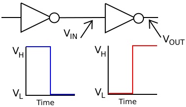

In an ideal world, the inverter circuit shown above would invert the signal instantaneously.

In the real world, gates don't transfer logic levels instantaneously. It takes a finite amount of time for electrons and holes to move through the semiconductor material. Okay, so typical CMOS gate propagation delays are less than 100 ps (pico seconds), but there are other delays in the real world circuit caused by parasitic resistance, capacitance, and inductance.
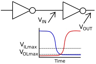
In the real world, a binary 0 is not represented by exactly zero volts. The above mentioned effects cause a binary low to be at some voltage below V(OLmax). When the output from the inverter gate on the left switches from high-to-low, the input of the inverter gate on the right won't recognize that switch until the voltage falls below V(ILmax). Only then will the second inverter begin to switch its output logic level from low to high.
| Specification | Description |
| V(IHmin) | Minimum input voltage that will be recognized as logic level 1 |
| V(ILmax) | Maximum input voltage that will be recognized as logic level 0 |
| V(OHmin) | Minimum output voltage for logic level 1 |
| V(OLmax) | Maximum output voltage for logic level 0 |
The actual voltages of these transfer characteristics depends upon the semiconductor type, family, and applied source voltage.

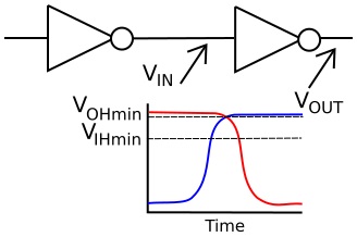
In the real world, a binary 1 is not represented by exactly the supply voltage. The above mentioned effects cause a binary 1 to be at some voltage above V(OHmin). In the circuit shown above, when the output of the inverter gate on the left switches from low-to-high, the input of the inverter gate on the right won't recognize that switch until the voltage falls below V(IHmin). Only then will the second inverter begin to switch its output logic level from high to low.

What if the output voltage of the inverter gate on the left begins to go low, achieves V(OLmax), but a transient causes the output voltage to spike above V(OLmax) before it drops back to V(OLmax)? The input of the inverter gate on the right would not see the transient as long as the voltage spike does not go above V(ILmax). It would switch its output to high as normal.
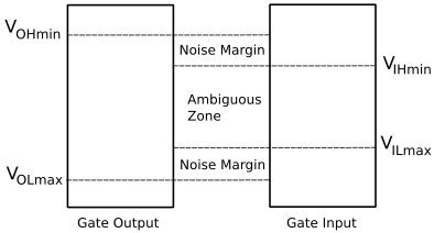
The voltage range between V(OLmax) and V(ILmax) is called the lower noise margin.
Similarly, what if the output voltage of the inverter gate on the left begins to go high and achieves V(OHmin), but then a transient causes the output voltage to spike below V(OHmin) before it rises back to V(OHmin)? The input of the inverter gate on the right would not see the transient as long as the voltage spike does not go below V(IHmin). It would switch its output to low as normal.
The voltage range between V(OHmin) and V(IHmin) is called the upper noise margin.
The real world is a noisy place (both audio wise and electrical wise), and if there were not noise margins built into all logic circuitry, there would be no reliable electronics in this world. But noise margins don't mean you can design electrically noisy circuits or operate circuitry in an electrically noisy environment without proper shielding. If the output voltage of the inverter above spends too muc time in the zone between V(ILmax) and V(IHmin), there is no predicting what the output of the inverter on the right will do. This is the ambiguous zone.
More Computer Architecture Articles:
• Operating System Memory Paging - Page Table Structure
• The Fetch, Decode, Execute Cycle
• Multiuser Operating System Functions
• Multi-Processor Scheduling
• Microprocessor Registers
• Virtual Memory and Memory Paging
• Integrated Circuit Design Flow
• AMD's Phenom Processor
• Basic Computer Architecture
• Intel's Dual-Core Core i3 Processor

